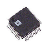
ADV7172KST Analog Devices Inc, ADV7172KST Datasheet - Page 23

ADV7172KST
Manufacturer Part Number
ADV7172KST
Description
Manufacturer
Analog Devices Inc
Datasheet
1.ADV7172KST.pdf
(60 pages)
Specifications of ADV7172KST
Number Of Dac's
6
Adc/dac Resolution
10b
Screening Level
Commercial
Package Type
LQFP
Pin Count
48
Lead Free Status / RoHS Status
Not Compliant
Available stocks
Company
Part Number
Manufacturer
Quantity
Price
Company:
Part Number:
ADV7172KST
Manufacturer:
SUN
Quantity:
5 000
Company:
Part Number:
ADV7172KST
Manufacturer:
ADI
Quantity:
850
Part Number:
ADV7172KST
Manufacturer:
ADI/亚德诺
Quantity:
20 000
Company:
Part Number:
ADV7172KSTZ
Manufacturer:
AD
Quantity:
80
Part Number:
ADV7172KSTZ
Manufacturer:
ADI/亚德诺
Quantity:
20 000
Company:
Part Number:
ADV7172KSTZ-REEL
Manufacturer:
Analog Devices Inc
Quantity:
10 000
POWER-ON RESET
After power-up, it is necessary to execute a reset operation. A
reset occurs on the falling edge of a high-to-low transition on
the RESET pin. This initializes the pixel port such that the pixel
inputs P7–P0 are not selected. After reset, the ADV7172/
ADV7173 is automatically set up to operate in NTSC/PAL mode,
depending on the PAL_NTSC pin. The subcarrier frequency
registers are automatically loaded with the correct values for
PAL or NTSC. All other registers, with the exception of Mode
Registers 1 and 2, are set to 00H. Mode Register 1 is set to 07H.
This is to ensure DACs D, E, and F are ON after power-up.
All bits of Mode Register 2 are set to “0,” with the exception of
Bit 3 (i.e., Mode Register 2 reads 08H). Bit MR23 of Mode
Register 2 is set to Logic “1.” This enables the 7.5 IRE pedestal.
RESET SEQUENCE
When RESET becomes active, the ADV7172/ADV7173 reverts
to the default output configuration. DACs A, B, C are off and
DACs D, E, F are powered on and output composite, luma and
chroma signals respectively. Mode Register 2, Bit 6 (MR26),
resets to “0.” The ADV7172/ADV7173 internal timing is under
the control of the logic level on the NTSC_PAL pin.
When RESET is released Y, Cr, Cb values corresponding to a
black screen are input to the ADV7172/ADV7173. Output
timing signals are still suppressed at this stage.
When the user requires valid data, MR26 is set to “1” to allow
the valid pixel data to pass through the encoder. Digital output
timing signals become active and the encoder timing is now
under the control of the timing registers. If, at this stage, the
user wishes to select a video standard different from that on the
NTSC_PAL pin, Mode Register 2, Bit 5 (MR25) is set (“1”)
and the video standard required is selected by programming
Mode Register 0. Figure 36 illustrates the reset sequence timing.
PIXEL DATA VALID
DIGITAL TIMING
COMPOSITE/Y
CHROMA
RESET
MR26
XXXXXXX
XXXXXXX
XXXXXXX
XXXXXXX
0
512
0
RESET
DIGITAL TIMING SIGNALS SUPPRESSED
SLEEP MODE
If after reset the SCRESET/RTC and NTSC_PAL pins are
both set to high, the part ADV7172/ADV7173 will power-up
in sleep mode to facilitate low power consumption before all
registers have been initialized. If Mode Register 6, Bit 0 (MR60) is
then set to (“1”) sleep mode control passes to Mode Register 2,
Bit 7 (i.e., control via I
SCH PHASE MODE
The SCH phase is configured in default mode to reset every
four (NTSC) or eight (PAL) fields to avoid an accumulation of
SCH phase error over time. In an ideal system, zero SCH phase
error would be maintained forever, but in reality, this is impos-
sible to achieve due to clock frequency variations. This effect is
reduced by the use of a 32-bit DDS, which generates this SCH.
Resetting the SCH phase every four or eight fields avoids the
accumulation of SCH phase error, and results in very minor
SCH phase jumps at the start of the four or eight field sequence.
Resetting the SCH phase should not be done if the video source
does not have stable timing or the ADV7172/ADV7173 is con-
figured in RTC mode (MR41 = “1” and MR42 = “1”). Under
these conditions (unstable video) the subcarrier phase reset should
be enabled (MR42 = “0” and MR41 = “1”) but no reset applied.
In this configuration the SCH phase will never be reset, which
that the output video will now track the unstable input video.
The subcarrier phase reset when applied will reset the SCH
phase to Field 0 at the start of the next field (e.g., subcarrier
phase reset applied in Field 5 (PAL) on the start of the next
field SCH phase will be reset to Field 0).
BLACK VALUE WITH SYNC
BLACK VALUE
2
C).
ADV7172/ADV7173
1
TIMING ACTIVE
VALID VIDEO
VALID VIDEO


