ADV7172KST Analog Devices Inc, ADV7172KST Datasheet - Page 7
ADV7172KST
Manufacturer Part Number
ADV7172KST
Description
Manufacturer
Analog Devices Inc
Datasheet
1.ADV7172KST.pdf
(60 pages)
Specifications of ADV7172KST
Number Of Dac's
6
Adc/dac Resolution
10b
Screening Level
Commercial
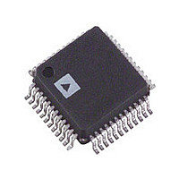
Package Type
LQFP
Pin Count
48
Lead Free Status / RoHS Status
Not Compliant
Available stocks
Company
Part Number
Manufacturer
Quantity
Price
Company:

Part Number:
ADV7172KST
Manufacturer:
SUN
Quantity:
5 000
Company:
Part Number:
ADV7172KST
Manufacturer:
ADI
Quantity:
850
Part Number:
ADV7172KST
Manufacturer:
ADI/亚德诺
Quantity:
20 000
Company:
Part Number:
ADV7172KSTZ
Manufacturer:
AD
Quantity:
80
Part Number:
ADV7172KSTZ
Manufacturer:
ADI/亚德诺
Quantity:
20 000
Company:
Part Number:
ADV7172KSTZ-REEL
Manufacturer:
Analog Devices Inc
Quantity:
10 000


3.3 V TIMING SPECIFICATIONS
Parameter
MPU PORT
ANALOG OUTPUTS
CLOCK CONTROL AND
PIXEL PORT
TELETEXT PORT
RESET CONTROL
NOTES
1
2
3
4
5
6
7
Specifications subject to change without notice.
The max/min specifications are guaranteed over this range. The max/min values are typical over 3.0 V to 3.6 V.
Temperature range T
TTL input values are 0 to 3 volts, with input rise/fall times ≤ 3 ns, measured between the 10% and 90% points. Timing reference points at 50% for inputs and
Guaranteed by characterization.
Output delay measured from the 50% point of the rising edge of CLOCK to the 50% point of full-scale transition.
Pixel Port consists of the following:
Teletext Port consists of the following:
outputs. Analog output load ≤ 10 pF.
Pixel Inputs:
Pixel Controls:
Clock Input:
Teletext Output:
Teletext Input:
SCLOCK Frequency
SCLOCK High Pulsewidth, t
SCLOCK Low Pulsewidth, t
Hold Time (Start Condition), t
Setup Time (Start Condition), t
Data Setup Time, t
SDATA, SCLOCK Rise Time, t
SDATA, SCLOCK Fall Time, t
Setup Time (Stop Condition), t
Analog Output Delay
DAC Analog Output Skew
f
Clock High Time, t
Clock Low Time, t
Data Setup Time, t
Data Hold Time, t
Control Setup Time, t
Control Hold Time, t
Digital Output Access Time, t
Digital Output Hold Time, t
Pipeline Delay, t
Digital Output Access Time, t
Data Setup Time, t
Data Hold Time, t
RESET Low Time
CLOCK
3, 4
4, 5, 6
MIN
15
P7–P0
HSYNC, FIELD/VSYNC, BLANK, VSO, CSO_HSO, CLAMP
CLOCK
TTXREQ
TTX
3, 4, 7
3, 4
12
18
to T
10
5
11
17
9
3, 5
12
MAX
11
: 0°C to 70°C.
14
2
1
13
16
3
8
4
7
6
Conditions
After this period the 1st clock is generated
relevant for repeated Start Condition.
(V
otherwise noted.)
AA
= 3.0 V–3.6 V
1
, V
REF
= 1.235 V, R
SET1,2
= 600
Min
0
0.6
1.3
0.6
0.6
100
0.6
8
8
4.0
5
5
3
. All specifications T
ADV7172/ADV7173
Typ
7
0
27
20
12
37
23
2
6
3
Max
400
300
300
MIN
to T
MAX
Unit
kHz
µs
µs
µs
µs
ns
ns
ns
µs
ns
ns
MHz
ns
ns
ns
ns
ns
ns
ns
ns
Clock Cycles
ns
ns
ns
ns
2
unless
Related parts for ADV7172KST
Image
Part Number
Description
Manufacturer
Datasheet
Request
R

Part Number:
Description:
±1.7g Dual-Axis IMEMS Accelerometer Evaluation Board
Manufacturer:
Analog Devices Inc
Datasheet:

Part Number:
Description:
Inertial Sensor Evaluation System
Manufacturer:
Analog Devices Inc
Datasheet:
Part Number:
Description:
Manufacturer:
Analog Devices Inc
Datasheet:
Part Number:
Description:
Manufacturer:
Analog Devices Inc
Datasheet:
Part Number:
Description:
Manufacturer:
Analog Devices Inc
Datasheet:
Part Number:
Description:
Manufacturer:
Analog Devices Inc
Datasheet:
Part Number:
Description:
Manufacturer:
Analog Devices Inc
Datasheet:
Part Number:
Description:
Manufacturer:
Analog Devices Inc
Datasheet:
Part Number:
Description:
Manufacturer:
Analog Devices Inc
Datasheet:
Part Number:
Description:
Manufacturer:
Analog Devices Inc
Datasheet:
Part Number:
Description:
Manufacturer:
Analog Devices Inc
Datasheet:
Part Number:
Description:
Manufacturer:
Analog Devices Inc
Datasheet:
Part Number:
Description:
Manufacturer:
Analog Devices Inc
Datasheet: