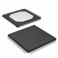
XC3S250E-4TQG144I Xilinx Inc, XC3S250E-4TQG144I Datasheet - Page 139

XC3S250E-4TQG144I
Manufacturer Part Number
XC3S250E-4TQG144I
Description
FPGA Spartan®-3E Family 250K Gates 5508 Cells 572MHz 90nm (CMOS) Technology 1.2V 144-Pin TQFP
Manufacturer
Xilinx Inc
Series
Spartan™-3Er
Datasheet
1.XC3S100E-4VQG100C.pdf
(233 pages)
Specifications of XC3S250E-4TQG144I
Package
144TQFP
Family Name
Spartan®-3E
Device Logic Cells
5508
Device Logic Units
612
Device System Gates
250000
Number Of Registers
4896
Maximum Internal Frequency
572 MHz
Typical Operating Supply Voltage
1.2 V
Maximum Number Of User I/os
108
Ram Bits
221184
Number Of Logic Elements/cells
5508
Number Of Labs/clbs
612
Total Ram Bits
221184
Number Of I /o
108
Number Of Gates
250000
Voltage - Supply
1.14 V ~ 1.26 V
Mounting Type
Surface Mount
Operating Temperature
-40°C ~ 100°C
Package / Case
144-LQFP
Lead Free Status / RoHS Status
Lead free / RoHS Compliant
For Use With
813-1009 - MODULE USB-TO-FPGA TOOL W/MANUAL
Lead Free Status / RoHS Status
Lead free / RoHS Compliant
Available stocks
Company
Part Number
Manufacturer
Quantity
Price
Company:
Part Number:
XC3S250E-4TQG144I
Manufacturer:
XILINX
Quantity:
1 670
Company:
Part Number:
XC3S250E-4TQG144I
Manufacturer:
XILINX
Quantity:
284
Company:
Part Number:
XC3S250E-4TQG144I
Manufacturer:
Xilinx Inc
Quantity:
10 000
Part Number:
XC3S250E-4TQG144I
Manufacturer:
XILINX/赛灵思
Quantity:
20 000
Table 99: CLB Distributed RAM Switching Characteristics
Table 100: CLB Shift Register Switching Characteristics
DS312-3 (v3.8) August 26, 2009
Product Specification
Clock-to-Output Times
Setup Times
Hold Times
Clock Pulse Width
Clock-to-Output Times
Setup Times
Hold Times
Clock Pulse Width
T
T
WPH
WPH
T
Symbol
Symbol
T
T
T
AH,
T
SHCKO
SRLDS
SRLDH
T
T
T
T
REG
WS
AS
DH
DS
, T
, T
T
WH
WPL
WPL
R
Time from the active edge at the CLK input to data
appearing on the distributed RAM output
Setup time of data at the BX or BY input before the active
transition at the CLK input of the distributed RAM
Setup time of the F/G address inputs before the active
transition at the CLK input of the distributed RAM
Setup time of the write enable input before the active
transition at the CLK input of the distributed RAM
Hold time of the BX, BY data inputs after the active
transition at the CLK input of the distributed RAM
Hold time of the F/G address inputs or the write enable
input after the active transition at the CLK input of the
distributed RAM
Minimum High or Low pulse width at CLK input
Time from the active edge at the CLK input to data
appearing on the shift register output
Setup time of data at the BX or BY input before the active
transition at the CLK input of the shift register
Hold time of the BX or BY data input after the active
transition at the CLK input of the shift register
Minimum High or Low pulse width at CLK input
Description
Description
www.xilinx.com
0.40
0.46
0.34
0.13
0.88
0.41
0.14
0.88
Min
Min
0
-
-
-5
-5
DC and Switching Characteristics
Max
2.05
Max
3.62
-
-
-
-
-
-
-
-
-
0.46
0.52
0.40
0.15
1.01
0.46
0.16
1.01
Min
Min
0
-
-
-4
-4
Max
2.35
Max
4.16
-
-
-
-
-
-
-
-
-
Units
Units
ns
ns
ns
ns
ns
ns
ns
ns
ns
ns
ns
139


