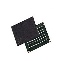
MT45W2MW16BGB-701 IT Micron Technology Inc, MT45W2MW16BGB-701 IT Datasheet - Page 29

MT45W2MW16BGB-701 IT
Manufacturer Part Number
MT45W2MW16BGB-701 IT
Description
Manufacturer
Micron Technology Inc
Datasheet
1.MT45W2MW16BGB-701_IT.pdf
(61 pages)
Specifications of MT45W2MW16BGB-701 IT
Operating Temperature (max)
85C
Operating Temperature (min)
-40C
Mounting
Surface Mount
Operating Temperature Classification
Industrial
Lead Free Status / RoHS Status
Compliant
Figure 22:
WAIT Polarity (BCR[10]) Default = WAIT Active HIGH
Latency Counter (BCR[13:11]) Default = Three-Clock Latency
Operating Mode (BCR[15]) Default = Asynchronous Operation
Table 5:
PDF: 09005aef82832fa2/Source: 09005aef82832f5f
32mb_burst_cr1_0_p24z_2.fm - Rev. E 9/08 EN
Latency Configuration Code
2 (3 clocks)
3 (4 clocks) – default
DQ[15:0]
WAIT
WAIT
CLK
Latency Configuration
WAIT Configuration During Burst Operation
Note:
The WAIT polarity bit indicates whether an asserted WAIT output should be HIGH or
LOW. This bit will determine whether the WAIT signal requires a pull-up or pull-down
resistor to maintain the deasserted state.
The latency counter bits determine how many clocks occur between the beginning of a
READ or WRITE operation and the first data value transferred. Only latency code 2 (3
clocks) or latency code 3 (4 clocks) is allowed (see Table 5 and Figure 23 on page 30).
The operating mode bit either selects synchronous burst operation or the default asyn-
chronous mode of operation.
Nondefault BCR setting for WAIT during BURST operation: WAIT active LOW.
D[0]
32Mb: 2 Meg x 16 Async/Page/Burst CellularRAM 1.0 Memory
D[1]
29
104 (9.62ns)
104 MHz
66 (15ns)
D[2]
Micron Technology, Inc., reserves the right to change products or specifications without notice.
Max Input CLK Frequency
D[3]
Configuration Registers
D[4]
Don’t Care
©2007 Micron Technology, Inc. All rights reserved.
53 (18.75ns)
80 (12.50ns)
BCR[8] = 0
Data valid in current cycle
BCR[8] = 1
Data valid in next cycle
80 MHz


