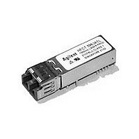
HFCT-5963NL Avago Technologies US Inc., HFCT-5963NL Datasheet - Page 8

HFCT-5963NL
Manufacturer Part Number
HFCT-5963NL
Description
Manufacturer
Avago Technologies US Inc.
Datasheet
1.HFCT-5963NL.pdf
(16 pages)
Specifications of HFCT-5963NL
Optical Fiber Type
TX/RX
Data Transfer Rate
155Mbps
Optical Rise Time
2ns
Optical Fall Time
2ns
Operating Temperature Classification
Commercial
Peak Wavelength
1360/1580nm
Package Type
DIP With Connector
Operating Supply Voltage (min)
3.1V
Operating Supply Voltage (typ)
3.3V
Operating Supply Voltage (max)
3.5V
Output Current
50mA
Operating Temp Range
-5C to 70C
Mounting
Snap Fit To Panel
Pin Count
10
Lead Free Status / RoHS Status
Compliant
Figure 6b. Recommended ac coupled interface circuit
The HFCT-5963TL/TG/NL/NG/ATL/ATG have a transmit
disable function which is a single-ended +3.3 V TTL input
which is dc-coupled to pin 8.
As for the receiver section, it is internally ac-coupled be-
tween the preamplifier and the postamplifier stages. The
actual Data and Data-bar outputs of the postamplifier are
dc-coupled to their respective output pins (pins 4, 5). The
two data outputs of the receiver should be terminated
with identical load circuits.
Signal Detect is a single-ended, +3.3 V TTL output signal
that is dc-coupled to pin 3 of the module. Signal Detect
should not be ac-coupled externally to the follow-on cir-
cuits because of its infrequent state changes.
Power Supply Filtering and Ground Planes
It is important to exercise care in circuit board layout to
achieve optimum performance from these transceiv-
ers. Figures 6a and 6b show the power supply circuit
which complies with the small form factor multisource
agreement. It is further recommended that a continuous
ground plane be provided in the circuit board directly
under the transceiver to provide a low inductance ground
for signal return current. This recommendation is in keep-
ing with good high frequency board layout practices.
8
T
Note: C1 = C2 = C3 = 10 nF or 100 nF
Note A: CIRCUIT ASSUMES OPEN EMITTER OUTPUT
Note B: WHEN INTERNAL BIAS IS PROVIDED REPLACE SPLIT RESISTORS WITH 100 W TERMINATION
* C4 AND C5 ARE OPTIONAL BYPASS CAPACITORS FOR ADDITIONAL LOW FREQUENCY NOISE FILTERING.
DIS
T
R
X
X
(LVTTL)
10
1
9
2
8
3
7
4
82 Ω
130 Ω
130 Ω
V
6
CC
5
(+3.3 V)
82 Ω
130 Ω
130 Ω
C2
C1
100 nF
1 µH
1 µH
100 nF
100 nF
100 nF
100 nF
C5 *
10 µF
C4 *
10 µF
Package footprint and front panel considerations
The Avago Technologies transceivers comply with the
circuit board “Common Transceiver Footprint” hole pat-
tern defined in the current multisource agreement which
defined the 2 x 5 package style. This drawing is reproduced
in Figure 7 with the addition of ANSI Y14.5M compliant
dimensioning to be used as a guide in the mechanical
layout of your circuit board. Figure 8 shows the front panel
dimensions associated with such a layout.
Eye Safety Circuit
For an optical transmitter device to be eye-safe in the
event of a single fault failure, the transmitter must either
maintain eye-safe operation or be disabled.
The HFCT-5963TL/TG/NL/NG/ATL/ATG is intrinsically eye
safe and does not require shut down circuitry.
Z = 50 Ω
Z = 50 Ω
Z = 50 Ω
Z = 50 Ω
Z = 50 Ω
V
CC
C3
(+3.3 V)
100 nF
10 µF
130 Ω
82 Ω
130 Ω
V
CC
82 Ω
130 Ω
(+3.3 V)
TD-
TD+
RD+
RD-
SD
130
Ω
LVTTL
V
CC
V
(+3.3 V)
CC
(+3.3 V)
NOTE A
NOTE B


