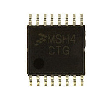
MC9S08SH4CTG Freescale, MC9S08SH4CTG Datasheet - Page 80

MC9S08SH4CTG
Manufacturer Part Number
MC9S08SH4CTG
Description
Manufacturer
Freescale
Datasheet
1.MC9S08SH4CTG.pdf
(338 pages)
Specifications of MC9S08SH4CTG
Cpu Family
HCS08
Device Core Size
8b
Frequency (max)
40MHz
Interface Type
I2C/SCI/SPI
Total Internal Ram Size
256Byte
# I/os (max)
13
Number Of Timers - General Purpose
1
Operating Supply Voltage (typ)
3.3/5V
Operating Supply Voltage (max)
5.5V
Operating Supply Voltage (min)
2.7V
On-chip Adc
8-chx10-bit
Instruction Set Architecture
CISC
Operating Temp Range
-40C to 85C
Operating Temperature Classification
Industrial
Mounting
Surface Mount
Pin Count
16
Package Type
TSSOP
Program Memory Type
Flash
Program Memory Size
4KB
Lead Free Status / RoHS Status
Compliant
Available stocks
Company
Part Number
Manufacturer
Quantity
Price
Company:
Part Number:
MC9S08SH4CTG
Manufacturer:
FREESCAL
Quantity:
96
Company:
Part Number:
MC9S08SH4CTG
Manufacturer:
Freescale
Quantity:
8 727
- Current page: 80 of 338
- Download datasheet (4Mb)
1
Chapter 6 Parallel Input/Output Control
6.6.1
Port A is controlled by the registers listed below.
The pins PTA4 and PTA5 are unique. PTA4 is output-only, so the control bits for the input function will
not have any effect on this pin. PTA5, when configured as an output, is open drain with low drive strength.
6.6.1.1
80
PTAD[5:0]
Reset:
Reads of bit PTAD4 always return the contents of PTAD4, regardless of the value stored in bit PTADD4.
Field
5:0
W
R
Port A Registers
Port A Data Register Bits — For port A pins that are inputs, reads return the logic level on the pin. For port A
pins that are configured as outputs, reads return the last value written to this register.
Writes are latched into all bits of this register. For port A pins that are configured as outputs, the logic level is
driven out the corresponding MCU pin.
Reset forces PTAD to all 0s, but these 0s are not driven out the corresponding pins because reset also configures
all port pins as high-impedance inputs with pull-ups/pull-downs disabled.
Port A Data Register (PTAD)
0
0
7
This PTA5 pin does not contain a clamp diode to V
driven above V
When the internal pullup device is enabled on PTA5 when used as an input
or open drain output the voltage measured on PTA5 will not be pulled to
V
pin is required to drive to a V
DD
. The internal gates connected to this pin are pulled to V
0
0
6
DD
Table 6-2. PTAD Register Field Descriptions
.
Figure 6-3. Port A Data Register (PTAD)
MC9S08SH8 MCU Series Data Sheet, Rev. 3
PTAD5
0
5
DD
PTAD4
level an external pullup should be used.
NOTE
0
4
1
Description
PTAD3
3
0
DD
and should not be
PTAD2
DD
0
2
. If the PTA5
Freescale Semiconductor
PTAD1
0
1
PTAD0
0
0
Related parts for MC9S08SH4CTG
Image
Part Number
Description
Manufacturer
Datasheet
Request
R

Part Number:
Description:
TOWER ELEVATOR BOARDS HARDWARE
Manufacturer:
Freescale Semiconductor
Datasheet:

Part Number:
Description:
TOWER SERIAL I/O HARDWARE
Manufacturer:
Freescale Semiconductor
Datasheet:

Part Number:
Description:
LCD MODULE FOR TWR SYSTEM
Manufacturer:
Freescale Semiconductor
Datasheet:

Part Number:
Description:
DAUGHTER LCD WVGA I.MX51
Manufacturer:
Freescale Semiconductor
Datasheet:

Part Number:
Description:
TOWER SYSTEM BOARD MPC5125
Manufacturer:
Freescale Semiconductor
Datasheet:

Part Number:
Description:
KIT EVALUATION I.MX51
Manufacturer:
Freescale Semiconductor
Datasheet:

Part Number:
Description:
KIT DEVELOPMENT WINCE IMX25
Manufacturer:
Freescale Semiconductor
Datasheet:

Part Number:
Description:
TOWER SYSTEM KIT MPC5125
Manufacturer:
Freescale Semiconductor
Datasheet:

Part Number:
Description:
TOWER SYSTEM BOARD K40X256
Manufacturer:
Freescale Semiconductor
Datasheet:

Part Number:
Description:
TOWER SYSTEM KIT K40X256
Manufacturer:
Freescale Semiconductor
Datasheet:

Part Number:
Description:
Microcontrollers (MCU) MX28 PLATFORM DEV KIT
Manufacturer:
Freescale Semiconductor
Datasheet:

Part Number:
Description:
MCU, MPU & DSP Development Tools IAR KickStart Kit for Kinetis K60
Manufacturer:
Freescale Semiconductor
Datasheet:

Part Number:
Description:
24BIT HDMI MX535/08
Manufacturer:
Freescale Semiconductor
Datasheet:
Part Number:
Description:
Manufacturer:
Freescale Semiconductor, Inc
Datasheet:
Part Number:
Description:
Manufacturer:
Freescale Semiconductor, Inc
Datasheet:


