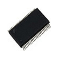
SSTV16857MTDX Fairchild Semiconductor, SSTV16857MTDX Datasheet - Page 2

SSTV16857MTDX
Manufacturer Part Number
SSTV16857MTDX
Description
Manufacturer
Fairchild Semiconductor
Datasheet
1.SSTV16857MTDX.pdf
(7 pages)
Specifications of SSTV16857MTDX
Logic Family
SSTV
Logical Function
Registered Buffer
Number Of Elements
1
Number Of Bits
14
Number Of Inputs
14
Number Of Outputs
14
High Level Output Current
-20mA
Low Level Output Current
20mA
Package Type
TSSOP
Propagation Delay Time
5ns
Operating Supply Voltage (typ)
2.5V
Operating Supply Voltage (max)
2.7V
Operating Supply Voltage (min)
2.3V
Clock-edge Trigger Type
Posit/Negat-Edge
Polarity
Non-Inverting
Technology
CMOS
Frequency (max)
200(Min)MHz
Mounting
Surface Mount
Pin Count
48
Operating Temp Range
0C to 70C
Operating Temperature Classification
Commercial
Output Type
Standard
Lead Free Status / RoHS Status
Compliant
www.fairchildsemi.com
Functional Description
The SSTV16857 and SSTVN16587 are 14-bit registers
with SSTL-2 compatible inputs and outputs. Input data is
captured by the register on the positive edge crossing of
the differential clock pair.
When the LV-CMOS RESET signal is asserted LOW, all
outputs and internal registers are asynchronously placed
into the LOW logic state. In addition, the clock and data dif-
ferential comparators are disabled for power savings. Out-
put glitches are prevented by disabling the internal
registers more quickly than the input comparators. When
Logic Diagram
2
RESET is removed, the system designer must insure the
clock and data inputs to the device are stable during the
rising transition of the RESET signal.
The SSTL-2 data inputs transition based on the value of
V
the trip point of the input buffers of the SSTV16857/
SSTVN16857 and other SSTL-2 compatible devices.
The RESET signal is a standard CMOS compatible input
and is not referenced to the V
REF
. V
REF
is a stable system reference used for setting
REF
signal.


