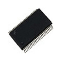
SSTV16857MTDX Fairchild Semiconductor, SSTV16857MTDX Datasheet - Page 5

SSTV16857MTDX
Manufacturer Part Number
SSTV16857MTDX
Description
Manufacturer
Fairchild Semiconductor
Datasheet
1.SSTV16857MTDX.pdf
(7 pages)
Specifications of SSTV16857MTDX
Logic Family
SSTV
Logical Function
Registered Buffer
Number Of Elements
1
Number Of Bits
14
Number Of Inputs
14
Number Of Outputs
14
High Level Output Current
-20mA
Low Level Output Current
20mA
Package Type
TSSOP
Propagation Delay Time
5ns
Operating Supply Voltage (typ)
2.5V
Operating Supply Voltage (max)
2.7V
Operating Supply Voltage (min)
2.3V
Clock-edge Trigger Type
Posit/Negat-Edge
Polarity
Non-Inverting
Technology
CMOS
Frequency (max)
200(Min)MHz
Mounting
Surface Mount
Pin Count
48
Operating Temp Range
0C to 70C
Operating Temperature Classification
Commercial
Output Type
Standard
Lead Free Status / RoHS Status
Compliant
f
t
t
(Note 5)
t
(Note 5)
t
t
t
t
t
t
f
t
t
(Note 5)
t
(Note 5)
t
t
t
t
t
t
t
MAX
W
ACT
INACT
S
H
REM
PHL
PHL
SK(Pn-Pn)
MAX
W
ACT
INACT
S
H
REM
PHL
PSS
PHL
SK(Pn-Pn)
AC Electrical Characteristics (SSTV16857)
Note 4: Refer to Figure 1 through Figure 7.
Note 5: This parameter is not production tested.
Note 6: For data signal input slew rate
Note 7: For data signal input slew rate
Note 8: For CK, CK signals input slew rates are
AC Electrical Characteristics (SSTVN16857)
Note 9: Refer to Figure 1 through Figure 7.
Note 10: This parameter is not production tested.
Note 11: For data signal input slew rate
Note 12: For data signal input slew rate
Note 13: For CK, CK signals input slew rates are
Note 14: Simultaneous Switching is guaranteed by characterization.
Symbol
Symbol
, t
, t
PLH
PLH
Maximum Clock Frequency
Pulse Duration, CK, CK HIGH or LOW (Figure 2)
Differential Inputs Activation Time,
data inputs must be LOW after RESET HIGH (Figure 3)
Differential Inputs De-activation Time,
data and clock inputs must be held at valid levels
(not floating) after RESET LOW
Setup Time, Fast Slew Rate (Note 6)(Note 7) (Figure 5)
Setup Time, Slow Slew Rate (Note 7)(Note 8) (Figure 5)
Hold Time, Fast Slew Rate (Note 6)(Note 8) (Figure 5)
Hold Time, Slow Slew Rate (Note 7)(Note 8) (Figure 5)
Reset Removal Time (Figure 7)
Propagation Delay CLK, CLK to Q
Propagation Delay RESET to Q
Output to Output Skew
Maximum Clock Frequency
Pulse Duration, CK, CK HIGH or LOW (Figure 2)
Differential Inputs Activation Time,
data inputs must be LOW after RESET HIGH (Figure 3)
Differential Inputs De-activation Time,
Data and Clock Inputs must be held at valid levels
(not floating) after RESET LOW
Setup Time, Fast Slew Rate (Note 9)(Note 12) (Figure 5)
Setup Time, Slow Slew Rate (Note 12)(Note 13) (Figure 5)
Hold Time, Fast Slew Rate (Note 11)(Note 13) (Figure 5)
Hold Time, Slow Slew Rate (Note 12)(Note 13) (Figure 5)
Reset Removal Time (Figure 7)
Propagation Delay CLK, CLK to Q
Propagation Delay Simultaneous Switching CLK, CLK to Q
Propagation Delay RESET to Q
Output to Output Skew
t
t
t
t
1 V/ns.
0.5 V/ns and
1 V/ns.
0.5 V/ns and
Parameter
Parameter
n
n
t
t
(Figure 6)
(Figure 6)
1 V/ns.
n
n
1 V/ns.
(Figure 4)
(Figure 4)
1 V/ns.
1 V/ns.
n
5
(Note 14)
(Note 4)
T
T
V
V
A
A
(Note 9)
DD
DD
0
0
q
q
C to
C to
2.5V
0.65
0.75
2.5V
0.65
0.75
0.75
Min
Min
200
220
2.5
0.9
0.9
1.1
2.5
0.9
1.1
22
22
10
22
22
10
r
r
70
70
0.2V; V
0.2V; V
q
q
C, C
C, C
L
L
DDQ
DDQ
30 pF, R
30 pF, R
2.5V
2.5V
Max
Max
200
200
2.8
5.0
2.4
2.7
5.0
L
L
r
r
www.fairchildsemi.com
0.2V
0.2V
50
50
:
:
Units
Units
MHz
MHz
ns
ns
ns
ns
ns
ns
ns
ns
ns
ns
ps
ns
ns
ns
ns
ns
ns
ns
ps


