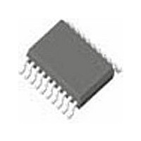
PI6C48543LE Pericom Semiconductor, PI6C48543LE Datasheet - Page 2

PI6C48543LE
Manufacturer Part Number
PI6C48543LE
Description
Clock Drivers & Distribution Fanout Buffer 3.3V
Manufacturer
Pericom Semiconductor
Type
Clock Driverr
Datasheet
1.PI6C48543LE.pdf
(6 pages)
Specifications of PI6C48543LE
Number Of Clock Inputs
2
Output Logic Level
LVDS
Mode Of Operation
Differential
Output Frequency
800MHz
Operating Supply Voltage (min)
3.135V
Operating Supply Voltage (typ)
3.3V
Operating Supply Voltage (max)
3.465V
Package Type
TSSOP
Operating Temp Range
-40C to 85C
Operating Temperature Classification
Industrial
Mounting
Surface Mount
Pin Count
20
Max Output Freq
800 MHz
Minimum Operating Temperature
- 40 C
Mounting Style
SMD/SMT
Number Of Outputs
16
Supply Current
60 mA
Supply Voltage (max)
3.465 V
Supply Voltage (min)
3.135 V
Maximum Operating Temperature
+ 85 C
Package / Case
TSSOP-20
Lead Free Status / RoHS Status
Compliant
Lead Free Status / RoHS Status
Lead free / RoHS Compliant, Compliant
Available stocks
Company
Part Number
Manufacturer
Quantity
Price
Company:
Part Number:
PI6C48543LE
Manufacturer:
PER
Quantity:
179
Part Number:
PI6C48543LEX
Manufacturer:
PERICOM
Quantity:
20 000
Pin Description
Notes:
1.
Pin Characteristics
Control Input Function Table
Notes:
1.
GND
CLK_EN
CLK_
SEL
CLK
n
PCLK
n
OE
V
Q
Q
Q
Q
CLK
PCLK
CC
3
2
1
0
Name
R_pulldown
,
,
,
,
I = Input, O = Output, P = Power supply connection, I_PD = Input with pull down, I_PU = Input with pull up
After CLK_EN switches, the clock outputs are disabled or enabled following a rising and falling input clock edge as show below.
R_pullup
n
n
n
n
Symbol
Q
Q
Q
Q
OE
C
1
1
1
1
0
08-0247
3
2
1
IN
1, 9, 13
10, 18
11, 12
14, 15
16, 17
19, 20
Pin #
2
3
4
5
6
7
8
Input Pulldown Resistance
CLK_EN
Input Pullup Resistance
Input Capacitance
0
0
1
1
x
Type
I_PU
I_PD
I_PD
I_PU
I_PD
I_PU
I_PU
O
O
O
O
P
P
Parameter
Connect to Ground
Synchronized clock enable. When high, clock outputs follow clock input. When low, Q
outputs are forced low,
Clock select input. When high, selects CLK
LVTTL level with 80kΩ pull down.
Non-inverting differential clock input
Inverting differential clock input
Non-inverting differential clock input
Inverting differential clock input
Output Enable, Controls outputs Q
Connect to 3.3V.
Differential output pair, LVDS interface level.
Differential output pair, LVDS interface level.
Differential output pair, LVDS interface level.
Differential output pair, LVDS interface level.
Inputs
CLK_SEL
0
1
0
1
x
Conditions
Selected Source
n
PCLK,
PCLK,
Q
CLK,
CLK,
x
outputs are forced high. LVCMOS/LVTTL level with 80kΩ pull up.
2
n
n
n
n
CLK
PCLK
CLK
PCLK
0
,
n
Q
0
through Q
Description
1
Min.
input. When low, selects CLK
Diasbled: Low
Disabled: Low
3
,
Differential to LVDS Fanout Buffer
Enabled
Enabled
Q
n
Hi-Z
Q
0
:Q
3.3V Low Skew 1-to-4, 800MHz,
3
3
Typ.
80
80
6
Outputs
Max.
Diasbled: High
Disabled: High
0
input. LVCMOS/
n
Enabled
Enabled
Q
Hi-Z
PS8771B
0
:
PI6C48543
n
Q
3
Units
x
kΩ
pF
10/02/08


