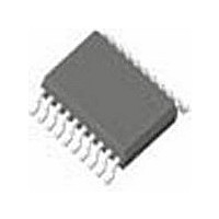
PI6C48543LE Pericom Semiconductor, PI6C48543LE Datasheet - Page 5

PI6C48543LE
Manufacturer Part Number
PI6C48543LE
Description
Clock Drivers & Distribution Fanout Buffer 3.3V
Manufacturer
Pericom Semiconductor
Type
Clock Driverr
Datasheet
1.PI6C48543LE.pdf
(6 pages)
Specifications of PI6C48543LE
Number Of Clock Inputs
2
Output Logic Level
LVDS
Mode Of Operation
Differential
Output Frequency
800MHz
Operating Supply Voltage (min)
3.135V
Operating Supply Voltage (typ)
3.3V
Operating Supply Voltage (max)
3.465V
Package Type
TSSOP
Operating Temp Range
-40C to 85C
Operating Temperature Classification
Industrial
Mounting
Surface Mount
Pin Count
20
Max Output Freq
800 MHz
Minimum Operating Temperature
- 40 C
Mounting Style
SMD/SMT
Number Of Outputs
16
Supply Current
60 mA
Supply Voltage (max)
3.465 V
Supply Voltage (min)
3.135 V
Maximum Operating Temperature
+ 85 C
Package / Case
TSSOP-20
Lead Free Status / RoHS Status
Compliant
Lead Free Status / RoHS Status
Lead free / RoHS Compliant, Compliant
Available stocks
Company
Part Number
Manufacturer
Quantity
Price
Company:
Part Number:
PI6C48543LE
Manufacturer:
PER
Quantity:
179
Part Number:
PI6C48543LEX
Manufacturer:
PERICOM
Quantity:
20 000
LVDS DC Characteristics
AC Characteristics
Notes:
1.
2
3.
4.
Applications Information
Wiring the differential input to accept single ended levels
Figure 1 shows how the differential input can be wired to accept single ended levels. The reference voltage V_REF = V
generated by the bias resistors R1, R2 and C1. This bias circuit should be located as close as possible to the input pin. The ratio of
R1 and R2 might need to be adjusted to postion the V_REF in the center of the input voltage swing. For example, if the input clock
swing is only 2.5V and V
f
t
Tsk(o)
Tsk(pp)
t
odc
Pd
r
max
V
∆V
V
∆V
I
I
I
I
V
V
Symbol
Symbol
/t
OZ
OFF
OSD
OS
f
OD
OS
OH
OL
Measured from the differenital input crossing point to the differential output crossing point
Skew between outputs with the same supply voltage and equal load conditions. Measured at the differential outputs crossing point.
Skew between outputs on different parts operating with the same supply voltage and equal load conditions. Measured at the differential out-
puts crossing point.
All parameters are measured at 500 MHz unless noted otherwise
OD
OS
08-0247
Differential Output Voltage
VOD Magnitude Change
Offset Voltage
VOS Magnitude Change
High Impedance Leakage Current
Power OFF Leakage
Differential Output Short Circuit Current
Output Short Circuit Current
Output Voltage High
Output Voltage Low
Output Frequency
Propagation Delay
Output-to-output Skew
Part-to-part Skew
Output Rise/Fall time
Output duty cycle
(T
DD
Parameter
A
= 3.3V, V_REF should be 1.25V and R1/R2 = 0.609.
= -40
Parameter
(3)
(1)
(T
o
C to 85
A
= -40
(2)
o
o
C, V
C to 85
CC
o
= 3.135V to 3.465V)
C, V
f ≤ 800 MHz
20% - 80%
CC
Conditions
= 3.135V to 3.465V unless otherwise stated below.)
5
Conditions
Min.
100
1.0
48
Differential to LVDS Fanout Buffer
3.3V Low Skew 1-to-4, 800MHz,
1.125
Min.
200
-10
-20
0.9
Typ.
Typ.
1.25
1.34
1.06
280
-3.5
-3.5
±1
0
5
Max.
800
300
300
2.2
40
52
1.375
Max.
+10
+20
360
1.6
40
25
PS8771B
-5
-5
PI6C48543
DD
/2 is
Units
MHz
ns
ps
%
Units
mV
mV
mA
μA
10/02/08
V
V


