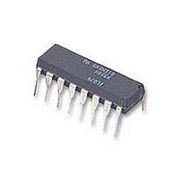
PCF8591P NXP Semiconductors, PCF8591P Datasheet - Page 14

PCF8591P
Manufacturer Part Number
PCF8591P
Description
IC, A/D AND D/A CONVERTER, 8BIT, 16-DIP
Manufacturer
NXP Semiconductors
Type
General Purposer
Specifications of PCF8591P
Number Of Channels
1
Number Of Adc's
1
Number Of Dac's
1
Adc/dac Resolution
8b
Interface Type
Serial (I2C)
Operating Supply Voltage (typ)
3.3/5V
Sample Rate
11.1KSPS
Number Of Adc Inputs
4
Number Of Dac Outputs
1
Operating Supply Voltage (max)
6V
Operating Supply Voltage (min)
2.5V
Operating Temperature (max)
85C
Operating Temperature (min)
-40C
Pin Count
16
Mounting
Through Hole
Supply Voltage Range
2.5V To 6V
Operating Temperature Range
-40°C To +85°C
Digital Ic Case Style
DIP
No. Of Pins
16
Linearity Error -
1.5LSB
Termination Type
DIP
Supply Voltage Max
8V
Input Channels Per Adc
1
Rohs Compliant
Yes
Filter Terminals
DIP
Conversion Time
90µs
Data Interface
I2C, Serial
Lead Free Status / RoHS Status
Compliant
Available stocks
Company
Part Number
Manufacturer
Quantity
Price
Company:
Part Number:
PCF8591P
Manufacturer:
SANYO
Quantity:
20 200
Company:
Part Number:
PCF8591P
Manufacturer:
NXP
Quantity:
5 510
Philips Semiconductors
8.5
After a start condition a valid hardware address has to be sent to a PCF8591 device. The read/write bit defines the
direction of the following single or multiple byte data transfer. For the format and the timing of the start condition (S), the
stop condition (P) and the acknowledge bit (A) refer to the I
terminated by sending either a stop condition or the start condition of the next data transfer.
2003 Jan 27
handbook, full pagewidth
handbook, full pagewidth
8-bit A/D and D/A converter
I
2
C-bus protocol
S
S
ADDRESS
ADDRESS
Fig.17 Bus protocol for read mode, A/D conversion.
Fig.16 Bus protocol for write mode, D/A conversion.
0
1
from PCF8591
from PCF8591
acknowledge
acknowledge
A
A
CONTROL BYTE
DATA BYTE
N = 0 to M
data bytes
14
2
from PCF8591
C-bus characteristics. In the write mode a data transfer is
acknowledge
acknowledge
from master
A
A
DATA BYTE
LAST DATA BYTE
N = 0 to M
data bytes
from PCF8591
acknowledge
A
no acknowledge
P/S
1
MBL833
MBL834
Product specification
P
PCF8591


