ICS9DB1200CGLF IDT, Integrated Device Technology Inc, ICS9DB1200CGLF Datasheet - Page 3
ICS9DB1200CGLF
Manufacturer Part Number
ICS9DB1200CGLF
Description
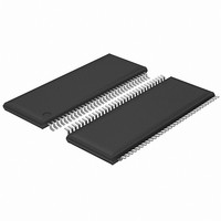
IC BUFFER 12OUTPUT DIFF 64-TSSOP
Manufacturer
IDT, Integrated Device Technology Inc
Type
Clock Bufferr
Series
-r
Datasheet
1.ICS9DB1200CGLFT.pdf
(14 pages)
Specifications of ICS9DB1200CGLF
Input
Differential
Output
Differential
Frequency - Max
400MHz
Voltage - Supply
3.135 V ~ 3.465 V
Operating Temperature
0°C ~ 70°C
Mounting Type
Surface Mount
Package / Case
64-TSSOP
Frequency-max
400MHz
Lead Free Status / RoHS Status
Lead free / RoHS Compliant
Other names
9DB1200CGLF
Available stocks
Company
Part Number
Manufacturer
Quantity
Price
Company:

Part Number:
ICS9DB1200CGLF
Manufacturer:
IDT
Quantity:
124
Part Number:
ICS9DB1200CGLF
Manufacturer:
IDT
Quantity:
20 000
Part Number:
ICS9DB1200CGLFT
Manufacturer:
IDT
Quantity:
20 000


Pin Description
IDT
PIN #
ICS9DB1200C
Twelve Output Differential Buffer for PCIe Gen1/Gen2, QPI, and FBDIMM
10
11
12
13
14
15
16
17
18
19
20
21
22
23
24
25
26
27
28
29
30
31
32
1
2
3
4
5
6
7
8
9
TM
/ICS
TM
VDD
DIF_IN
DIF_IN#
GND
OE0#
DIF_0
DIF_0#
VDD
GND
OE1#
DIF_1
DIF_1#
OE2#
DIF_2
DIF_2#
GND
VDD
OE3#
DIF_3
DIF_3#
OE4#
DIF_4
DIF_4#
VDD
GND
OE5#
DIF_5
DIF_5#
**ADR_SEL
HIGH_BW#
FS2
SMBCLK
Twelve Output Differential Buffer for PCIe Gen1/Gen2, QPI, and FBDIMM
PIN NAME
TYPE
PWR
PWR
OUT
OUT
PWR
PWR
OUT
OUT
OUT
OUT
PWR
PWR
OUT
OUT
OUT
OUT
PWR
PWR
OUT
OUT
IN
IN
IN
IN
IN
IN
IN
IN
IN
IN
IN
IN
Power supply, nominal 3.3V
0.7 V Differential TRUE input
0.7 V Differential Complementary Input
Ground pin.
Active low input for enabling DIF pair 0.
1 = tri-state outputs, 0 = enable outputs
0.7V differential true clock output
0.7V differential Complementary clock output
Power supply, nominal 3.3V
Ground pin.
Active low input for enabling DIF pair 1.
1 = tri-state outputs, 0 = enable outputs
0.7V differential true clock output
0.7V differential Complementary clock output
Active low input for enabling DIF pair 2.
1 = tri-state outputs, 0 = enable outputs
0.7V differential true clock output
0.7V differential Complementary clock output
Ground pin.
Power supply, nominal 3.3V
Active low input for enabling DIF pair 3.
1 = tri-state outputs, 0 = enable outputs
0.7V differential true clock output
0.7V differential Complementary clock output
Active low input for enabling DIF pair 4
1 = tri-state outputs, 0 = enable outputs
0.7V differential true clock output
0.7V differential Complementary clock output
Power supply, nominal 3.3V
Ground pin.
Active low input for enabling DIF pair 5.
1 = tri-state outputs, 0 = enable outputs
0.7V differential true clock output
0.7V differential Complementary clock output
This tri-level input selects one of 3 SMBus addresses. See the SMBus
Address Select Table for the addresses.
3.3V input for selecting PLL Band Width
0 = High, 1= Low
Frequency select pin.
Clock pin of SMBUS circuitry, 5V tolerant
3
DESCRIPTION
1414E—11/04/09
Related parts for ICS9DB1200CGLF
Image
Part Number
Description
Manufacturer
Datasheet
Request
R

Part Number:
Description:
TRANSLATION DEVICE DPI 80-PQFP
Manufacturer:
IDT, Integrated Device Technology Inc
Datasheet:
Part Number:
Description:
IDT PART
Manufacturer:
IDT, Integrated Device Technology Inc
Datasheet:
Part Number:
Description:
IC LIU T1/E1/J1 OCTAL 256PBGA
Manufacturer:
IDT, Integrated Device Technology Inc
Datasheet:

Part Number:
Description:
IC FREQ TIMING GENERATOR 28TSSOP
Manufacturer:
IDT, Integrated Device Technology Inc
Datasheet:
Part Number:
Description:
IC CLK DVR PLL 1:10 40VFQFPN
Manufacturer:
IDT, Integrated Device Technology Inc
Datasheet:
Part Number:
Description:
IC CLK FANOUT BUFFER 1:18 32LQFP
Manufacturer:
IDT, Integrated Device Technology Inc
Datasheet:
Part Number:
Description:
IC CLK FANOUT BUFFER 1:18 32LQFP
Manufacturer:
IDT, Integrated Device Technology Inc
Datasheet:
Part Number:
Description:
IC CK505 VREG/RES 56TSSOP
Manufacturer:
IDT, Integrated Device Technology Inc
Datasheet:

Part Number:
Description:
IC SDRAM CLK DVR 1:10 48-TSSOP
Manufacturer:
IDT, Integrated Device Technology Inc
Datasheet:

Part Number:
Description:
IC CLK DVR PLL 1:10 48TSSOP
Manufacturer:
IDT, Integrated Device Technology Inc
Datasheet:
Part Number:
Description:
IC FLEXPC CLK PROGR P4 56-TSSOP
Manufacturer:
IDT, Integrated Device Technology Inc
Datasheet:
Part Number:
Description:
IC FLEXPC CLK PROGR P4 56-TSSOP
Manufacturer:
IDT, Integrated Device Technology Inc
Datasheet:
Part Number:
Description:
IC FLEXPC CLK PROGR P4 56-SSOP
Manufacturer:
IDT, Integrated Device Technology Inc
Datasheet:

Part Number:
Description:
IC PLL CLK DRIVER 2.5V 28-TSSOP
Manufacturer:
IDT, Integrated Device Technology Inc
Datasheet:
Part Number:
Description:
IC CLOCK DRIVER 2.5V 24-TSSOP
Manufacturer:
IDT, Integrated Device Technology Inc
Datasheet: