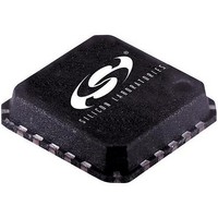
SI5010-BM Silicon Laboratories Inc, SI5010-BM Datasheet - Page 12

SI5010-BM
Manufacturer Part Number
SI5010-BM
Description
IC CLOCK/DATA RECOVERY LP 20MLP
Manufacturer
Silicon Laboratories Inc
Type
Clock and Data Recovery (CDR)r
Datasheet
1.SI5010-BM.pdf
(20 pages)
Specifications of SI5010-BM
Package / Case
20-VQFN Exposed Pad, 20-HVQFN, 20-SQFN, 20-DHVQFN
Input
LVTTL
Output
CML
Frequency - Max
666MHz
Voltage - Supply
2.375 V ~ 2.625 V
Operating Temperature
-40°C ~ 85°C
Mounting Type
Surface Mount
Frequency-max
666MHz
Product
RF / Wireless
Maximum Operating Temperature
85 C
Minimum Operating Temperature
- 40 C
Mounting Style
SMD/SMT
Lead Free Status / RoHS Status
Contains lead / RoHS non-compliant
Other names
336-1120
Si5010
4.10. Differential Input Circuitry
The Si5010 provides differential inputs for both the high-speed data (DIN) and the reference clock (REFCLK)
inputs. An example termination for these inputs is shown in Figure 6. In applications where direct dc coupling is
possible, the 0.1 µF capacitors may be omitted. The DIN and REFCLK input amplifiers require an input signal with
a minimum differential peak-to-peak voltage listed in Table 2 on page 6.
12
Differential
Driver
Clock
source
Clock
source
Figure 7. Single-Ended Input Termination for REFCLK (AC Coupled)
Figure 8. Single-Ended Input Termination for DIN (AC Coupled)
Figure 6. Input Termination for DIN and REFCLK (AC Coupled)
0.1 µF
0.1 µF
Zo = 50 ¬
Zo = 50 ¬
0.1 µF
0.1 µF
Zo = 50 Ω
Zo = 50 Ω
REFCLK+
REFCLK–
0.1 µF
0.1 µF
100 Ω
100 Ω
DIN+,
DIN–,
Rev. 1.3
2.5 k¬
10 k¬
REFCLK +
REFCLK –
DIN +
DIN –
Si5010
2.5 k¬
2.5 kΩ
2.5 kΩ
10 kΩ
10 kΩ
10 k¬
VDD
GND
Si5010
Si5010
GND
GND
VDD
2.5 kΩ
VDD
2.5 kΩ
10 kΩ
10 kΩ
102 ¬
102 Ω
102 Ω


