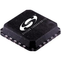
SI5010-BM Silicon Laboratories Inc, SI5010-BM Datasheet - Page 15

SI5010-BM
Manufacturer Part Number
SI5010-BM
Description
IC CLOCK/DATA RECOVERY LP 20MLP
Manufacturer
Silicon Laboratories Inc
Type
Clock and Data Recovery (CDR)r
Datasheet
1.SI5010-BM.pdf
(20 pages)
Specifications of SI5010-BM
Package / Case
20-VQFN Exposed Pad, 20-HVQFN, 20-SQFN, 20-DHVQFN
Input
LVTTL
Output
CML
Frequency - Max
666MHz
Voltage - Supply
2.375 V ~ 2.625 V
Operating Temperature
-40°C ~ 85°C
Mounting Type
Surface Mount
Frequency-max
666MHz
Product
RF / Wireless
Maximum Operating Temperature
85 C
Minimum Operating Temperature
- 40 C
Mounting Style
SMD/SMT
Lead Free Status / RoHS Status
Contains lead / RoHS non-compliant
Other names
336-1120
Pin #
12
13
15
16
17
19
20
PWRDN/CAL
CLKOUT+
Pin Name
CLKOUT–
RATESEL
DOUT+
DOUT–
NC
Table 8. Si5010 Pin Descriptions (Continued)
I/O
O
O
I
I
Signal Level
LVTTL
LVTTL
CML
CML
Rev. 1.3
Differential Data Output.
The data output signal is a retimed version of the
data recovered from the signal present on DIN. It is
phase aligned with CLKOUT and is updated on the
rising edge of CLKOUT.
Powerdown.
To shut down the high-speed outputs and reduce
power consumption, hold this pin high. For normal
operation, hold this pin low.
Calibration.
To initiate an internal self-calibration, force a
high-to-low transition on this pin. (See "4.2. PLL
Self-Calibration" on page 10.)
Note: This input has a weak internal pulldown.
Differential Clock Output.
The output clock is recovered from the data signal
present on DIN. In the absence of data, the output
clock is derived from REFCLK.
Data Rate Select.
This pin configures the onboard PLL for clock and
data recovery at one of two user selectable data
rates. See Table 7 for configuration settings.
Note: This input has a weak internal pulldown.
No Connect.
This pin should be tied to ground.
Description
Si5010
15


