SI5010-BM Silicon Laboratories Inc, SI5010-BM Datasheet - Page 17
SI5010-BM
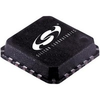
Manufacturer Part Number
SI5010-BM
Description
IC CLOCK/DATA RECOVERY LP 20MLP
Manufacturer
Silicon Laboratories Inc
Type
Clock and Data Recovery (CDR)r
Datasheet
1.SI5010-BM.pdf
(20 pages)
Specifications of SI5010-BM
Package / Case
20-VQFN Exposed Pad, 20-HVQFN, 20-SQFN, 20-DHVQFN
Input
LVTTL
Output
CML
Frequency - Max
666MHz
Voltage - Supply
2.375 V ~ 2.625 V
Operating Temperature
-40°C ~ 85°C
Mounting Type
Surface Mount
Frequency-max
666MHz
Product
RF / Wireless
Maximum Operating Temperature
85 C
Minimum Operating Temperature
- 40 C
Mounting Style
SMD/SMT
Lead Free Status / RoHS Status
Contains lead / RoHS non-compliant
Other names
336-1120


8. Package Outline: Si5010-BM/GM
Figure 11 illustrates the package details for the Si5010-BM/GM. Table 9 lists the values for the dimensions shown
in the illustration.
0.50 DIA.
PIN1 ID
Notes:
Symbol
D, E
1. Dimensioning and tolerances conform to ASME Y14.5M. - 1994
2. Package warpage MAX 0.05 mm.
3. “b” applies to plated terminal and is measured between 0.20 and 0.25 mm from terminal TIP.
4. The package weight is approximately 42 mg.
5. The mold compound for this package has a flammability rating of UL94-V0 with an oxygen index of 28
6. The recommended reflow profile for this package is defined by the JEDEC-020B Small Body specification.
A1
A2
A3
A
b
1
2
3
minimum/54 typical.
20
Top View
0.00
0.18
Min
D1
—
—
D
Millimeters
0.20 REF.
4.00 BSC
Nom
Figure 11. 20-pin Quad Flat No-Lead (QFN)
0.85
0.01
0.65
0.23
E1
Table 9. Package Dimensions
E
Max
0.90
0.05
0.70
0.30
θ
A2
Rev. 1.3
A
Side View
Symbol
b
e
A1
A3
D1, E1
D2, E2
e
L
θ
0.50
1.95
Min
—
e
L
b
Bottom View
Millimeters
3.75 BSC
0.50 BSC
Nom
2.10
0.60
—
D2
20
Si5010
Max
2.25
0.75
12°
1
2
3
E2
17
Related parts for SI5010-BM
Image
Part Number
Description
Manufacturer
Datasheet
Request
R

Part Number:
Description:
BOARD EVALUATION FOR SI5010
Manufacturer:
Silicon Laboratories Inc
Datasheet:

Part Number:
Description:
IC CLOCK/DATA RECOVERY LP 20-QFN
Manufacturer:
Silicon Laboratories Inc
Datasheet:
Part Number:
Description:
Clock and Data Recovery 20-Pin QFN EP T/R
Manufacturer:
Silicon Laboratories Inc
Datasheet:

Part Number:
Description:
Telecom ICs SONET/SDH 2.5 V OC-3/12 STM-1/4
Manufacturer:
Silicon Laboratories Inc
Datasheet:
Part Number:
Description:
SMD/C°/SINGLE-ENDED OUTPUT SILICON OSCILLATOR
Manufacturer:
Silicon Laboratories Inc
Part Number:
Description:
Manufacturer:
Silicon Laboratories Inc
Datasheet:
Part Number:
Description:
N/A N/A/SI4010 AES KEYFOB DEMO WITH LCD RX
Manufacturer:
Silicon Laboratories Inc
Datasheet:
Part Number:
Description:
N/A N/A/SI4010 SIMPLIFIED KEY FOB DEMO WITH LED RX
Manufacturer:
Silicon Laboratories Inc
Datasheet:
Part Number:
Description:
N/A/-40 TO 85 OC/EZLINK MODULE; F930/4432 HIGH BAND (REV E/B1)
Manufacturer:
Silicon Laboratories Inc
Part Number:
Description:
EZLink Module; F930/4432 Low Band (rev e/B1)
Manufacturer:
Silicon Laboratories Inc
Part Number:
Description:
I°/4460 10 DBM RADIO TEST CARD 434 MHZ
Manufacturer:
Silicon Laboratories Inc
Part Number:
Description:
I°/4461 14 DBM RADIO TEST CARD 868 MHZ
Manufacturer:
Silicon Laboratories Inc
Part Number:
Description:
I°/4463 20 DBM RFSWITCH RADIO TEST CARD 460 MHZ
Manufacturer:
Silicon Laboratories Inc
Part Number:
Description:
I°/4463 20 DBM RADIO TEST CARD 868 MHZ
Manufacturer:
Silicon Laboratories Inc