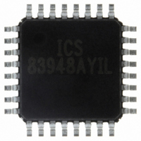
ICS83948AYILF IDT, Integrated Device Technology Inc, ICS83948AYILF Datasheet - Page 4

ICS83948AYILF
Manufacturer Part Number
ICS83948AYILF
Description
IC FANOUT BUFFER 1:12 32-LQFP
Manufacturer
IDT, Integrated Device Technology Inc
Series
HiPerClockS™r
Type
Fanout Buffer (Distribution), Multiplexerr
Datasheet
1.ICS83948AYILF.pdf
(13 pages)
Specifications of ICS83948AYILF
Number Of Circuits
1
Ratio - Input:output
2:12
Differential - Input:output
Yes/No
Input
HCSL, LVCMOS, LVDS, LVHSTL, LVPECL, LVTTL, SSTL
Output
LVCMOS, LVTTL
Frequency - Max
250MHz
Voltage - Supply
3 V ~ 3.6 V
Operating Temperature
-40°C ~ 85°C
Mounting Type
Surface Mount
Package / Case
32-LQFP
Frequency-max
250MHz
Lead Free Status / RoHS Status
Lead free / RoHS Compliant
Other names
800-1120
83948AYILF
83948AYILF
Available stocks
Company
Part Number
Manufacturer
Quantity
Price
Company:
Part Number:
ICS83948AYILF
Manufacturer:
IDT
Quantity:
231
Company:
Part Number:
ICS83948AYILF
Manufacturer:
IDT, Integrated Device Technology Inc
Quantity:
10 000
Company:
Part Number:
ICS83948AYILFT
Manufacturer:
IDT, Integrated Device Technology Inc
Quantity:
10 000
Table 4B. DC Characteristics, V
NOTE 1: V
NOTE 2: Common mode voltage is defined as V
AC Electrical Characteristics
Table 5. AC Characteristics, V
NOTE 1A: Measured from the differential input crossing point to V
NOTE 1B: Measured from V
NOTE 2: Defined as skew between outputs at the same supply voltage and with equal load conditions. Measured at V
NOTE 3: Defined as skew between outputs on different devices operating a the same supply voltage and with equal load conditions.
Using the same type of inputs on each device, the outputs are measured at V
NOTE 4: These parameters are guaranteed by characterization. Not tested in production.
NOTE 5: Setup and Hold times are relative to the rising edge of the input clock.
NOTE 6: This parameter is defined in accordance with JEDEC Standard 65.
IDT™ / ICS™ LVCMOS/LVTTL CLOCK GENERATOR
Symbol
V
V
V
V
I
V
V
Parameter
f
t
tsk(o)
tsk(pp)
t
t
t
t
t
t
IN
MAX
PD
R
PW
PZL,
PLZ,
S
H
ICS83948I
LOW SKEW, 1-TO-12 DIFFERENTIAL-TO-LVCMOS/LVTTL FANOUT BUFFER
IH
IL
PP
CMR
OH
OL
/ t
F
t
t
PZH
PHZ
IL
Parameter
Input High Voltage
Input Low Voltage
Peak-to-Peak Input Voltage; NOTE 1
Common Mode Input Voltage; NOTE 1, 2
Input Current
Output High Voltage
Output Low Voltage
should not be less than -0.3V.
Symbol
Output Frequency
Propagation Delay
Output Skew; NOTE 2, 6
Part-to-Part Skew;
NOTE 3, 6
Output Rise/Fall Time
Output Pulse Width
Output Enable Time; NOTE 4
Output Disable Time; NOTE 4
Clock Enable
Setup Time;
NOTE 5
Clock Enable
Hold Time;
NOTE 5
DD
/2 or crosspoint of the input to V
DD
CLK/nCLK;
NOTE 1A
LVCMOS_CLK;
NOTE 1B
CLK/nCLK
LVCMOS_CLK
CLK_EN to
CLK/nCLK
CLK_EN to
LVCMOS_CLK
CLK/nCLK to
CLK_EN
LVCMOS_CLK to
CLK_EN
DD
= V
= V
DDO
DDO
= 3.3V ± 0.3V, T
IH
= 3.3V ± 0.3V, T
.
Rising Edge @ V
Rising Edge @ V
Test Conditions
Measured on
Measured on
ƒ < 150MHz
ƒ ≤ 150MHz
ƒ ≤ 150MHz
DDO
Test Conditions
0.8V to 2V
I
A
DDO
I
OH
OL
/2 of the output.
A
4
= -40°C to 85°C
= -40°C to 85°C
= -20mA
= 20mA
/2 of the output.
DDO
DDO
DDO
/2
/2
/2.
t
Cycle
Minimum
GND + 0.5
Minimum
2.25
0.2
/2 - 800
2
1
0
1
1
0.15
-0.3
2.5
2
ICS83948AYI REV. C NOVEMBER 7, 2008
Typical
Typical
t
Cycle
V
Maximum
Maximum
V
DD
DD
±100
3.75
250
350
1.5
1.0
/2 + 800
0.8
1.3
0.4
11
11
DDO
4
2
– 0.85
+ 0.3
/2.
Units
Units
MHz
µA
V
V
V
V
V
V
ns
ns
ns
ps
ns
ns
ps
ns
ns
ns
ns
ns
ns


