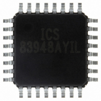
ICS83948AYILF IDT, Integrated Device Technology Inc, ICS83948AYILF Datasheet - Page 7

ICS83948AYILF
Manufacturer Part Number
ICS83948AYILF
Description
IC FANOUT BUFFER 1:12 32-LQFP
Manufacturer
IDT, Integrated Device Technology Inc
Series
HiPerClockS™r
Type
Fanout Buffer (Distribution), Multiplexerr
Datasheet
1.ICS83948AYILF.pdf
(13 pages)
Specifications of ICS83948AYILF
Number Of Circuits
1
Ratio - Input:output
2:12
Differential - Input:output
Yes/No
Input
HCSL, LVCMOS, LVDS, LVHSTL, LVPECL, LVTTL, SSTL
Output
LVCMOS, LVTTL
Frequency - Max
250MHz
Voltage - Supply
3 V ~ 3.6 V
Operating Temperature
-40°C ~ 85°C
Mounting Type
Surface Mount
Package / Case
32-LQFP
Frequency-max
250MHz
Lead Free Status / RoHS Status
Lead free / RoHS Compliant
Other names
800-1120
83948AYILF
83948AYILF
Available stocks
Company
Part Number
Manufacturer
Quantity
Price
Company:
Part Number:
ICS83948AYILF
Manufacturer:
IDT
Quantity:
231
Company:
Part Number:
ICS83948AYILF
Manufacturer:
IDT, Integrated Device Technology Inc
Quantity:
10 000
Company:
Part Number:
ICS83948AYILFT
Manufacturer:
IDT, Integrated Device Technology Inc
Quantity:
10 000
Application Information
Wiring the Differential Input to Accept Single Ended Levels
Figure 1 shows how the differential input can be wired to accept
single ended levels. The reference voltage V_REF = V
generated by the bias resistors R1, R2 and C1. This bias circuit
should be located as close as possible to the input pin. The ratio of
R1 and R2 might need to be adjusted to position the V_REF in the
center of the input voltage swing. For example, if the input clock
swing is only 2.5V and V
R2/R1 = 0.609.
Recommendations for Unused Input and Output Pins
Inputs:
CLK/nCLK Inputs
For applications not requiring the use of the differential input, both
CLK and nCLK can be left floating. Though not required, but for
additional protection, a 1kΩ resistor can be tied from CLK to
ground.
CLK Input
For applications not requiring the use of a clock input, it can be left
floating. Though not required, but for additional protection, a 1kΩ
resistor can be tied from the CLK input to ground.
LVCMOS Control Pins
All control pins have internal pull-ups or pull-downs; additional
resistance is not required but can be added for additional
protection. A 1kΩ resistor can be used.
IDT™ / ICS™ LVCMOS/LVTTL CLOCK GENERATOR
ICS83948I
LOW SKEW, 1-TO-12 DIFFERENTIAL-TO-LVCMOS/LVTTL FANOUT BUFFER
DD
= 3.3V, V_REF should be 1.25V and
DD
/2 is
7
Figure 1. Single-Ended Signal Driving Differential Input
Outputs:
LVCMOS Outputs
All unused LVCMOS output can be left floating. There should be no
trace attached.
Single Ended Clock Input
C1
0.1u
V_REF
ICS83948AYI REV. C NOVEMBER 7, 2008
R1
1K
R2
1K
V
DD
CLK
nCLK


