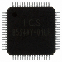
ICS8534AY-01LF IDT, Integrated Device Technology Inc, ICS8534AY-01LF Datasheet - Page 15

ICS8534AY-01LF
Manufacturer Part Number
ICS8534AY-01LF
Description
IC FANOUT BUFFER LVPECL 64-TQFP
Manufacturer
IDT, Integrated Device Technology Inc
Series
HiPerClockS™r
Type
Fanout Buffer (Distribution), Multiplexerr
Datasheet
1.ICS8534AY-01LF.pdf
(21 pages)
Specifications of ICS8534AY-01LF
Number Of Circuits
1
Ratio - Input:output
2:22
Differential - Input:output
Yes/Yes
Input
CML, HCSL, LVDS, LVHSTL, LVPECL, SSTL
Output
LVPECL
Frequency - Max
500MHz
Voltage - Supply
3.135 V ~ 3.465 V
Operating Temperature
0°C ~ 85°C
Mounting Type
Surface Mount
Package / Case
64-TQFP, 64-VQFP
Frequency-max
500MHz
Lead Free Status / RoHS Status
Lead free / RoHS Compliant
Other names
800-1173
8534AY-01LF
8534AY-01LF
Available stocks
Company
Part Number
Manufacturer
Quantity
Price
Company:
Part Number:
ICS8534AY-01LF
Manufacturer:
IDT
Quantity:
83
Company:
Part Number:
ICS8534AY-01LF
Manufacturer:
IDT, Integrated Device Technology Inc
Quantity:
10 000
Company:
Part Number:
ICS8534AY-01LFT
Manufacturer:
IDT, Integrated Device Technology Inc
Quantity:
10 000
ICS8534-01 Data Sheet
Power Considerations
This section provides information on power dissipation and junction temperature for the ICS8534-01.
Equations and example calculations are also provided.
1.
The total power dissipation for the ICS8534-01 is the sum of the core power plus the power dissipated in the load(s).
The following is the power dissipation for V
NOTE: Please refer to Section 3 for details on calculating power dissipated in the load.
Total Power_
2. Junction Temperature.
Junction temperature, Tj, is the temperature at the junction of the bond wire and bond pad directly affects the reliability of the device. The
maximum recommended junction temperature is 125°C. Limiting the internal transistor junction temperature, Tj, to 125°C ensures that the bond
wire and bond pad temperature remains below 125°C.
In order to calculate junction temperature, the appropriate junction-to-ambient thermal resistance θ
flow of 200 linear feet per minute and a multi-layer board, the appropriate value is 17.2°C/W per Table 6 below.
Therefore, Tj for an ambient temperature of 85°C with all outputs switching is:
This calculation is only an example. Tj will obviously vary depending on the number of loaded outputs, supply voltage, air flow and the type of
board (multi-layer).
Table 6. Thermal Resistance
ICS8534AY-01 REVISION B MARCH 28, 2011
Linear Feet per Minute
Multi-Layer PCB, JEDEC Standard Test Boards
Power Dissipation.
•
•
Power (core)
Power (outputs)
If all outputs are loaded, the total power is 22 * 30mW = 660mW
The equation for Tj is as follows: Tj = θ
Tj = Junction Temperature
θ
Pd_total = Total Device Power Dissipation (example calculation is in section 1 above)
T
85°C + 1.457W * 17.2°C/W = 110.1°C. This is below the limit of 125°C.
JA
A
= Ambient Temperature
= Junction-to-Ambient Thermal Resistance
MAX
(3.465V, with all outputs switching) = 796.95mW + 660mW = 1456.95mW
MAX
MAX
= V
= 30mW/Loaded Output pair
CC_MAX
θ
JA
* I
for 64 Lead TQFP, Forced Convection
EE_MAX
CC
= 3.465V, which gives worst case results.
JA
= 3.465V * 230mA = 796.95mW
* Pd_total + T
θ
JA
A
22.3°C/W
by Velocity
15
0
LOW SKEW, 1-TO-22 DIFFERENTIAL-TO-3.3V LVPECL FANOUT BUFFER
17.2°C/W
200
JA
must be used. Assuming a moderate air
©2011 Integrated Device Technology, Inc.
15.1°C/W
500


