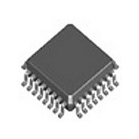
MPC9447AC IDT, Integrated Device Technology Inc, MPC9447AC Datasheet - Page 8

MPC9447AC
Manufacturer Part Number
MPC9447AC
Description
IC CLK FANOUT BUFFER 1:9 32-LQFP
Manufacturer
IDT, Integrated Device Technology Inc
Type
Fanout Buffer (Distribution), Multiplexerr
Datasheet
1.MPC9447ACR2.pdf
(10 pages)
Specifications of MPC9447AC
Number Of Circuits
1
Ratio - Input:output
2:9
Differential - Input:output
No/No
Input
LVCMOS
Output
LVCMOS
Frequency - Max
350MHz
Voltage - Supply
2.375 V ~ 3.465 V
Operating Temperature
-40°C ~ 85°C
Mounting Type
Surface Mount
Package / Case
32-LQFP
Frequency-max
350MHz
Number Of Clock Inputs
2
Mode Of Operation
Single-Ended
Output Frequency
350MHz
Output Logic Level
LVCMOS
Operating Supply Voltage (min)
2.375V
Operating Supply Voltage (typ)
2.5/3.3V
Operating Supply Voltage (max)
3.465V
Package Type
TQFP
Operating Temp Range
-40C to 85C
Operating Temperature Classification
Industrial
Signal Type
LVCMOS
Mounting
Surface Mount
Pin Count
32
Quiescent Current
2mA
Lead Free Status / RoHS Status
Lead free / RoHS Compliant
Available stocks
Company
Part Number
Manufacturer
Quantity
Price
Company:
Part Number:
MPC9447AC
Manufacturer:
IDT, Integrated Device Technology Inc
Quantity:
10 000
Company:
Part Number:
MPC9447ACR2
Manufacturer:
IDT, Integrated Device Technology Inc
Quantity:
10 000
MPC9447 Data Sheet
MPC9447 REVISION 6 APRIL 13, 2010
The variation in cycle time of a signal between adjacent cycles,
over a random sample of adjacent cycle pairs.
The time from the output controlled edge to the non-controlled edge,
divided by the time between output controlled edges, expressed as
a percentage.
The pin-to-pin skew is defined as the worst case difference in
propagation delay between any similar delay path within a single
device.
Figure 9. Output-to-Output Skew t
Figure 11. Output Duty Cycle (DC)
Figure 13. Cycle-to-Cycle Jitter
T
N
t
P
T
N+1
T
DC = (t
0
t
SK(LH)
P ?
T
T
0
JIT(CC)
x 100%)
Figure 8. Propagation Delay (t
CCLK
= |T
Q
SK(LH, HL)
N
X
t
SK(HL)
-T
N+1
V
V
GND
|
CC
CC
V
V
GND
V
V
GND
÷2
CC
CC
CC
CC
t
P(LH)
÷2
÷2
8
t
P(HL)
PD
Figure 14. Setup and Hold Time (t
Figure 10. Output Pulse Skew (t
) Test Reference
CLK_STOP
Figure 12. Output Transition Time Test Reference
CCLK
Q
t
CCLK
PCLK
F
X
V
V
GND
V
V
GND
CC
CC
CC
CC
÷2
÷2
t
P(LH)
3.3V, 2.5V, 1:9 LVCMOS CLOCK FANOUT BUFFER
t
SK(P)
t
= | t
S
©2010 Integrated Device Technology, Inc.
PLH
t
t
H
t
– t
R
P(HL)
PHL
SK(P)
V
S
|
CC
, t
0.55
=3.3 V
2.4
H
) Test Reference
) Test Reference
V
CC
1.8 V
0.6 V
=2.5 V
V
V
GND
V
V
GND
CC
CC
CC
CC
÷2
÷2
V
V
GND
V
V
GND
CC
CC
CC
CC
÷2
÷2


