ICS8533AGI-01LF IDT, Integrated Device Technology Inc, ICS8533AGI-01LF Datasheet
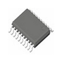
IC FANOUT BUFFER 1-4 20-TSSOP

ICS8533AGI-01LF

Manufacturer Part Number
ICS8533AGI-01LF
Description
IC FANOUT BUFFER 1-4 20-TSSOP
Manufacturer
IDT, Integrated Device Technology Inc
Type
Fanout Buffer (Distribution), Multiplexerr
Series
HiPerClockS™r
Datasheet

Specifications of ICS8533AGI-01LF

Number Of Circuits
1
Ratio - Input:output
2:4
Differential - Input:output
Yes/Yes
Input
CML, HCSL, LVDS, LVHSTL, LVPECL, SSTL
Output
LVPECL
Frequency - Max
650MHz
Voltage - Supply
3.135 V ~ 3.465 V
Operating Temperature
-40°C ~ 85°C
Mounting Type
Surface Mount
Package / Case
20-TSSOP
Frequency-max
650MHz
Number Of Clock Inputs
2
Mode Of Operation
Differential
Output Frequency
650MHz
Output Logic Level
LVPECL
Operating Supply Voltage (min)
3.135V
Operating Supply Voltage (typ)
3.3V
Operating Supply Voltage (max)
3.465V
Package Type
TSSOP
Operating Temp Range
-40C to 85C
Operating Temperature Classification
Industrial
Mounting
Surface Mount
Pin Count
20
Lead Free Status / RoHS Status
Lead free / RoHS Compliant
Other names
8533AGI-01LF

Available stocks

Company
Part Number
Manufacturer
Quantity
Price
Part Number:
ICS8533AGI-01LF
Manufacturer:
IDT
Quantity:
1 000
Part Number:
ICS8533AGI-01LF
Manufacturer:
IDT
Quantity:
300
Part Number:
ICS8533AGI-01LFT
Manufacturer:
SAMSUNG
Quantity:
40 000
B
8533AGI-01
G
inputs. The CLK, nCLK pair can accept most standard dif-
ferential input levels. The PCLK, nPCLK pair can accept
LVPECL, CML, or SSTL input levels. The clock enable is
internally synchronized to eliminate runt pulses on the out-
puts during asynchronous assertion/deassertion of the clock
enable pin.
Guaranteed output and part-to-part skew characteristics
make the ICS8533I-01 ideal for those applications demand-
ing well defined performance and repeatability.
HiPerClockS™
IC S
LOCK
ENERAL
CLK_SEL
CLK_EN
nPCLK
PCLK
nCLK
CLK
D
The ICS8533I-01 is a low skew, high perfor-
mance 1-to-4 Differential-to-3.3V LVPECL
Fanout Buffer and a member of the HiPerClockS™
family of High Performance Clock Solutions from
IDT. The ICS8533I-01 has two selectable clock
IAGRAM
D
ESCRIPTION
0
1
D
LE
Q
Q0
nQ0
Q1
nQ1
Q2
nQ2
Q3
nQ3
D
IFFERENTIAL
1
F
P
Four differential 3.3V LVPECL outputs
Selectable differential CLK, nCLK or LVPECL clock inputs
CLK, nCLK pair can accept the following differential
input levels: LVDS, LVPECL, LVHSTL, SSTL, HCSL
PCLK, nPCLK supports the following input types:
LVPECL, CML, SSTL
Maximum output frequency: 650MHz
Translates any single-ended input signal to 3.3V
LVPECL levels with resistor bias on nCLK input
Output skew: 30ps (maximum)
Part-to-part skew: 150ps (maximum)
Propagation delay: 1.5ns (maximum), CLK/nCLK
Additive phase jitter, RMS: 0.060ps (typical)
3.3V operating supply
-40°C to 85°C ambient operating temperature
Available in both standard (RoHS5) and lead-free (RoHS 6)
packages
EATURES
IN
A
SSIGNMENT
-
6.5mm x 4.4mm x 0.92mm package body
TO
-3.3V LVPECL F
CLK_SEL
CLK_EN
nPCLK
PCLK
nCLK
CLK
V
V
nc
nc
CC
ICS8533I-01
EE
20-Lead TSSOP
G Package
Top View
1
2
3
4
5
6
7
8
9
10
20
19
18
17
16
15
14
13
12
11
ICS8533I-01
L
OW
Q0
nQ0
V
Q1
nQ1
Q2
nQ2
V
Q3
nQ3
CC
CC
ANOUT
S
REV. A DECEMBER 6, 2007
KEW
, 1-
B
UFFER
TO
-4

Related parts for ICS8533AGI-01LF

ICS8533AGI-01LF Summary of contents

Page 1

G D ENERAL ESCRIPTION The ICS8533I- low skew, high perfor mance 1-to-4 Differential-to-3.3V LVPECL HiPerClockS™ Fanout Buffer and a member of the HiPerClockS™ family of High Performance Clock Solutions from IDT. The ICS8533I-01 has two selectable ...

Page 2

ABLE IN ESCRIPTIONS ...

Page 3

T 3A ABLE ONTROL NPUT UNCTION ...

Page 4

BSOLUTE AXIMUM ATINGS Supply Voltage Inputs Outputs Continuous Current Surge Current Package Thermal Impedance, JA Storage Temperature, T STG T 4A ABLE OWER UPPLY HARACTERISTICS S y ...

Page 5

T 4D. LVPECL DC C ABLE HARACTERISTICS ...

Page 6

The spectral purity in a band at a specific offset from the fun- damental compared to the power of the fundamental is called the dBc Phase Noise. This value is normally expressed using a Phase noise plot and is most ...

Page 7

P ARAMETER LVPECL V EE -1.3V ± 0.165 3. UTPUT OAD EST IRCUIT nQx Qx nQy Qy tsk( UTPUT KEW 80% Clock 20% Outputs ...

Page 8

IRING THE IFFERENTIAL NPUT TO Figure 2 shows how the differential input can be wired to accept single ended levels. The reference voltage V_REF = V generated by the bias resistors R1, R2 and C1. This bias ...

Page 9

IFFERENTIAL LOCK NPUT NTERFACE The CLK /nCLK accepts LVDS, LVPECL, LVHSTL, SSTL, HCSL and other differential signals. Both V the V and V input requirements. Figures show PP CMR interface examples for the ...

Page 10

LVPECL LOCK NPUT NTERFACE The PCLK /nPCLK accepts LVPECL, CML, SSTL and other differential signals. Both V and V SWING and V input requirements. Figures show inter- CMR face examples for the HiPerClockS PCLK/nPCLK ...

Page 11

T LVPECL O ERMINATION FOR UTPUTS The clock layout topology shown below is a typical termina- tion for LVPECL outputs. The two different layouts mentioned are recommended only as guidelines. FOUT and nFOUT are low impedance follower outputs that generate ...

Page 12

This section provides information on power dissipation and junction temperature for the ICS8533I-01. Equations and example calculations are also provided. 1. Power Dissipation. The total power dissipation for the ICS8533I-01 is the sum of the core power plus the power ...

Page 13

Calculations and Equations. The purpose of this section is to derive the power dissipated into the load. LVPECL output driver circuit and termination are shown in Figure calculate worst case power dissipation into the load, ...

Page 14

ABLE VS IR LOW ABLE FOR JA Single-Layer PCB, JEDEC Standard Test Boards Multi-Layer PCB, JEDEC Standard Test Boards NOTE: Most modern PCB designs use multi-layered boards. The data in the second row pertains ...

Page 15

ACKAGE UTLINE UFFIX FOR T Reference Document: JEDEC Publication 95, MS-153 8533AGI-01 D IFFERENTIAL TSSOP EAD ABLE ACKAGE IMENSIONS ...

Page 16

ABLE RDERING NFORMATION ...

Page 17

...

Related keywords