MAX9312ECJ+ Maxim Integrated Products, MAX9312ECJ+ Datasheet - Page 6
MAX9312ECJ+
Manufacturer Part Number
MAX9312ECJ+
Description
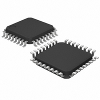
IC DVR CLK/DATA DUAL 1:5 32LQFP
Manufacturer
Maxim Integrated Products
Type
Fanout Buffer (Distribution), Datar
Datasheet
1.MAX9312ETJ.pdf
(9 pages)
Specifications of MAX9312ECJ+
Number Of Circuits
2
Ratio - Input:output
1:5
Differential - Input:output
Yes/Yes
Input
HSTL, LVECL, LVPECL
Output
LVECL, LVPECL
Frequency - Max
3GHz
Voltage - Supply
2.25 V ~ 3.8 V
Operating Temperature
-40°C ~ 85°C
Mounting Type
Surface Mount
Package / Case
32-LQFP
Frequency-max
3GHz
Lead Free Status / RoHS Status
Lead free / RoHS Compliant


Dual 1:5 Differential LVPECL/LVECL/HSTL
Clock and Data Drivers
6
1, 9, 16, 25, 32
_______________________________________________________________________________________
PIN
10
11
12
13
14
15
17
18
19
20
21
22
23
24
26
27
28
29
30
31
—
2
3
4
5
6
7
8
NAME
CLKA
CLKA
CLKB
CLKB
N.C.
QB4
QB4
QB3
QB3
QB2
QB2
QB1
QB1
QB0
QB0
QA4
QA4
QA3
QA3
QA2
QA2
QA1
QA1
QA0
QA0
V
V
V
EP
CC
BB
EE
Positive Supply Voltage. Bypass from V
Place the capacitors as close to the device as possible with the smaller value capacitor closest to
the device.
No Connection. Internally not connected.
Noninverting Differential Clock Input A
Inverting Differential Clock Input A
Reference Output Voltage. Connect to the inverting or noninverting clock input to provide a
reference for single-ended operation. When used, bypass to V
capacitor.
Noninverting Differential Clock Input B
Inverting Differential Clock Input B
Negative Supply Voltage
Inverting QB4 Output. Typically terminate with 50Ω resistor to V
Noninverting QB4 Output. Typically terminate with 50Ω resistor to V
Inverting QB3 Output. Typically terminate with 50Ω resistor to V
Noninverting QB3 Output. Typically terminate with 50Ω resistor to V
Inverting QB2 Output. Typically terminate with 50Ω resistor to V
Noninverting QB2 Output. Typically terminate with 50Ω resistor to V
Inverting QB1 Output. Typically terminate with 50Ω resistor to V
Noninverting QB1 Output. Typically terminate with 50Ω resistor to V
Inverting QB0 Output. Typically terminate with 50Ω resistor to V
Noninverting QB0 Output. Typically terminate with 50Ω resistor to V
Inverting QA4 Output. Typically terminate with 50Ω resistor to V
Noninverting QA4 Output. Typically terminate with 50Ω resistor to V
Inverting QA3 Output. Typically terminate with 50Ω resistor to V
Noninverting QA3 Output. Typically terminate with 50Ω resistor to V
Inverting QA2 Output. Typically terminate with 50Ω resistor to V
Noninverting QA2 Output. Typically terminate with 50Ω resistor to V
Inverting QA1 Output. Typically terminate with 50Ω resistor to V
Noninverting QA1 Output. Typically terminate with 50Ω resistor to V
Inverting QA0 Output. Typically terminate with 50Ω resistor to V
Noninverting QA0 Output. Typically terminate with 50Ω resistor to V
Exposed Pad (TQFN package only). Internally connected to V
the PCB.
CC
to V
FUNCTION
EE
with 0.1µF and 0.01µF ceramic capacitors.
EE
CC
CC
CC
CC
CC
CC
CC
CC
CC
CC
CC
. Connect EP to the V
with a 0.01µF ceramic
- 2V.
- 2V.
- 2V.
- 2V.
- 2V.
- 2V.
- 2V.
- 2V.
- 2V.
- 2V.
CC
CC
CC
CC
CC
CC
CC
CC
CC
CC
- 2V.
- 2V.
- 2V.
- 2V.
- 2V.
- 2V.
- 2V.
- 2V.
- 2V.
- 2V.
Pin Description
EE
pad on
Related parts for MAX9312ECJ+
Image
Part Number
Description
Manufacturer
Datasheet
Request
R

Part Number:
Description:
Manufacturer:
Maxim Integrated Products
Datasheet:

Part Number:
Description:
Ultra Low-Power, Low-Cost Comparators with 2eference
Manufacturer:
MAXIM [Maxim Integrated Products]
Datasheet:
Part Number:
Description:
MAX7528KCWPMaxim Integrated Products [CMOS Dual 8-Bit Buffered Multiplying DACs]
Manufacturer:
Maxim Integrated Products
Datasheet:
Part Number:
Description:
Single +5V, fully integrated, 1.25Gbps laser diode driver.
Manufacturer:
Maxim Integrated Products
Datasheet:
Part Number:
Description:
Single +5V, fully integrated, 155Mbps laser diode driver.
Manufacturer:
Maxim Integrated Products
Datasheet:
Part Number:
Description:
VRD11/VRD10, K8 Rev F 2/3/4-Phase PWM Controllers with Integrated Dual MOSFET Drivers
Manufacturer:
Maxim Integrated Products
Datasheet:
Part Number:
Description:
Highly Integrated Level 2 SMBus Battery Chargers
Manufacturer:
Maxim Integrated Products
Datasheet:
Part Number:
Description:
Current Monitor and Accumulator with Integrated Sense Resistor; ; Temperature Range: -40°C to +85°C
Manufacturer:
Maxim Integrated Products
Part Number:
Description:
TSSOP 14/A°/RS-485 Transceivers with Integrated 100O/120O Termination Resis
Manufacturer:
Maxim Integrated Products
Part Number:
Description:
TSSOP 14/A°/RS-485 Transceivers with Integrated 100O/120O Termination Resis
Manufacturer:
Maxim Integrated Products
Part Number:
Description:
QFN 16/A°/AC-DC and DC-DC Peak-Current-Mode Converters with Integrated Step
Manufacturer:
Maxim Integrated Products
Part Number:
Description:
TDFN/A/65V, 1A, 600KHZ, SYNCHRONOUS STEP-DOWN REGULATOR WITH INTEGRATED SWI
Manufacturer:
Maxim Integrated Products
Part Number:
Description:
Integrated Temperature Controller f
Manufacturer:
Maxim Integrated Products
Part Number:
Description:
SOT23-6/I°/45MHz to 650MHz, Integrated IF VCOs with Differential Output
Manufacturer:
Maxim Integrated Products
Part Number:
Description:
SOT23-6/I°/45MHz to 650MHz, Integrated IF VCOs with Differential Output
Manufacturer:
Maxim Integrated Products