MAX9325EQI+ Maxim Integrated Products, MAX9325EQI+ Datasheet - Page 10
MAX9325EQI+
Manufacturer Part Number
MAX9325EQI+
Description
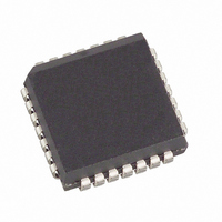
IC DRIVER DIFF 2:8 28-PLCC
Manufacturer
Maxim Integrated Products
Type
Fanout Buffer (Distribution), Multiplexer , Datar
Datasheet
1.MAX9325EQI.pdf
(12 pages)
Specifications of MAX9325EQI+
Number Of Circuits
1
Ratio - Input:output
2:8
Differential - Input:output
Yes/Yes
Input
HSTL, LVECL, LVPECL
Output
LVECL, LVPECL
Frequency - Max
700MHz
Voltage - Supply
2.375 V ~ 3.8 V
Operating Temperature
-40°C ~ 85°C
Mounting Type
Surface Mount
Package / Case
28-LCC, 28-PLCC
Frequency-max
700MHz
Lead Free Status / RoHS Status
Lead free / RoHS Compliant


2:8 Differential LVPECL/LVECL/HSTL Clock and
Data Driver
ferential input is configured for single-ended operation
by connecting the on-chip reference voltage, V
unused complementary input as a reference. For exam-
ple, the differential CLK0, CLK0 input is converted to a
noninverting, single-ended input by connecting V
CLK0 and connecting the single-ended input to CLK0.
Similarly, an inverting input is obtained by connecting
V
CLK0. With a differential input configured as single-
ended (using V
to V
signal.
When configuring a differential input as a single-ended
input, a user must ensure that the supply voltage (V
V
high minimum level must be at (V
for proper operation. The reference voltage V
be at least (V
because it becomes the high-level input when the other
single-ended input swings below it. The minimum V
output for the MAX9325 is (V
the minimum V
in a minimum supply (V
to standard supplies gives the single-ended operating
supply ranges (V
MAX9325.
When using the V
0.01µF ceramic capacitor to V
open. The V
which is sufficient to drive two inputs.
Terminate the outputs through 50Ω to (V
equivalent Thevenin terminations. Terminate each Q and
Q output with identical termination on each for low output
distortion. When a single-ended signal is taken from the
differential output, terminate both Q_ and Q_.
Ensure that output currents do not exceed the current
limits as specified in the Absolute Maximum Ratings
table. Under all operating conditions, the device’s total
thermal limits should be observed.
Bypass each V
mount ceramic 0.1µF and 0.01µF capacitors. Place the
capacitors as close to the device as possible with the
0.01µF capacitor closest to the device pins.
Use multiple vias when connecting the bypass capaci-
tors to ground. When using the V
bypass it with a 0.01µF ceramic capacitor to V
V
10
BB
EE
BB
) is greater than 2.58V. This is because the input
CC
reference is not used, it can be left open.
______________________________________________________________________________________
to CLK0 and connecting the single-ended input to
or V
EE
BB
EE
BB
BB
CC
or with a single-ended LVPECL/LVECL
Applications Information
reference can source or sink 0.5mA,
+ 1.2V) or higher for the same reason
), the single-ended input can be driven
BB
output for (V
CC
to V
reference output, bypass it with a
- V
CC
EE
EE
with high-frequency surface-
- V
) of 3.0V to 3.8V for the
EE
CC
Output Termination
BB
CC
) of 2.58V. Rounding up
Supply Bypassing
- 1.38V). Substituting
. If not used, leave it
= V
BB
EE
EE
+ 1.2V) or higher
reference output,
CC
+ 1.2V) results
- 2V) or use
CC
BB
BB
, to an
. If the
BB
must
CC
BB
to
-
Circuit board trace layout is very important to maintain
the signal integrity of high-speed differential signals.
Maintaining integrity is accomplished in part by reduc-
ing signal reflections and skew, and increasing com-
mon-mode noise immunity.
Signal reflections are caused by discontinuities in the
50Ω characteristic impedance of the traces. Avoid dis-
continuities by maintaining the distance between differ-
ential traces, not using sharp corners or using vias.
Maintaining distance between the traces also increases
common-mode noise immunity. Reducing signal skew
is accomplished by matching the electrical length of
the differential traces.
The 28-lead QFN package (MAX9325EGI) has the
exposed paddle on the bottom of the package that pro-
vides the primary heat removal path from the IC to the
PC board, as well as excellent electrical grounding to
the PC board. The MAX9325EGI’s exposed pad is
internally connected to V
exposed pad to a separate circuit ground plane
unless V
TRANSISTOR COUNT: 1030
PROCESS: Bipolar
CLK_SEL
CLK0
CLK0
CLK1
CLK1
EE
V
and the circuit ground are the same.
EE
V
V
EE
EE
75kΩ
105kΩ
105kΩ
MAX9325
Functional Diagram
Exposed-Pad Package
Chip Information
EE
0
1
. Do not connect the
Traces
Q0
Q0
Q1
Q1
Q2
Q2
Q3
Q3
Q4
Q4
Q5
Q5
Q6
Q6
Q7
Q7
Related parts for MAX9325EQI+
Image
Part Number
Description
Manufacturer
Datasheet
Request
R

Part Number:
Description:
Max9325 2 8 Differential Lvpecl/lvecl/hstl Clock And Data Driver
Manufacturer:
Maxim Integrated Products, Inc.
Datasheet:

Part Number:
Description:
MAX7528KCWPMaxim Integrated Products [CMOS Dual 8-Bit Buffered Multiplying DACs]
Manufacturer:
Maxim Integrated Products
Datasheet:
Part Number:
Description:
Single +5V, fully integrated, 1.25Gbps laser diode driver.
Manufacturer:
Maxim Integrated Products
Datasheet:
Part Number:
Description:
Single +5V, fully integrated, 155Mbps laser diode driver.
Manufacturer:
Maxim Integrated Products
Datasheet:
Part Number:
Description:
VRD11/VRD10, K8 Rev F 2/3/4-Phase PWM Controllers with Integrated Dual MOSFET Drivers
Manufacturer:
Maxim Integrated Products
Datasheet:
Part Number:
Description:
Highly Integrated Level 2 SMBus Battery Chargers
Manufacturer:
Maxim Integrated Products
Datasheet:
Part Number:
Description:
Current Monitor and Accumulator with Integrated Sense Resistor; ; Temperature Range: -40°C to +85°C
Manufacturer:
Maxim Integrated Products
Part Number:
Description:
TSSOP 14/A�/RS-485 Transceivers with Integrated 100O/120O Termination Resis
Manufacturer:
Maxim Integrated Products
Part Number:
Description:
TSSOP 14/A�/RS-485 Transceivers with Integrated 100O/120O Termination Resis
Manufacturer:
Maxim Integrated Products
Part Number:
Description:
QFN 16/A�/AC-DC and DC-DC Peak-Current-Mode Converters with Integrated Step
Manufacturer:
Maxim Integrated Products
Part Number:
Description:
TDFN/A/65V, 1A, 600KHZ, SYNCHRONOUS STEP-DOWN REGULATOR WITH INTEGRATED SWI
Manufacturer:
Maxim Integrated Products
Part Number:
Description:
Integrated Temperature Controller f
Manufacturer:
Maxim Integrated Products
Part Number:
Description:
SOT23-6/I�/45MHz to 650MHz, Integrated IF VCOs with Differential Output
Manufacturer:
Maxim Integrated Products
Part Number:
Description:
SOT23-6/I�/45MHz to 650MHz, Integrated IF VCOs with Differential Output
Manufacturer:
Maxim Integrated Products
Part Number:
Description:
EVALUATION KIT/2.4GHZ TO 2.5GHZ 802.11G/B RF TRANSCEIVER WITH INTEGRATED PA
Manufacturer:
Maxim Integrated Products