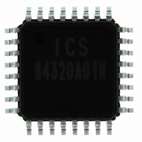
ICS84320AY-01LN IDT, Integrated Device Technology Inc, ICS84320AY-01LN Datasheet

ICS84320AY-01LN
Specifications of ICS84320AY-01LN
84320AY-01LN
Available stocks
Related parts for ICS84320AY-01LN
ICS84320AY-01LN Summary of contents
Page 1
G D ENERAL ESCRIPTION The ICS84320- general purpose, dual output Crystal- to-3.3V Differential LVPECL High Frequency Synthesizer. The ICS84320-01 has a selectable TEST_CLK or crystal inputs. The VCO operates at a frequency range of 620MHz to 780MHz. The ...
Page 2
F D UNCTIONAL ESCRIPTION NOTE: The functional description that follows describes op- eration using a 25MHz crystal. Valid PLL loop divider values for different crystal or input frequencies are defined in the In- put Frequency Characteristics, Table 5, NOTE 1. ...
Page 3
ABLE IN ESCRIPTIONS ...
Page 4
T 3A ABLE ARALLEL AND ERIAL ODE ...
Page 5
BSOLUTE AXIMUM ATINGS Supply Voltage Inputs, V -0. Outputs, V (LVCMOS) -0. Outputs, I (LVPECL) O Continuous Current 50mA Surge Current 100mA Package Thermal Impedance, θ Lead ...
Page 6
T 4C. LVPECL DC C ABLE HARACTERISTICS ...
Page 7
T 0 -10 -20 -30 -40 -50 -60 -70 -80 -90 -100 -110 -120 -130 -140 -150 -160 -170 -180 -10 -20 -30 -40 -50 -60 -70 -80 -90 -100 -110 -120 -130 -140 -150 -160 ...
Page 8
P ARAMETER CCO CCA LVPECL V EE -1.3V ± 0.165V 3. UTPUT OAD EST IRCUIT 1σ contains 68.26% of all measurements 2σ contains 95.4% of all measurements 3σ ...
Page 9
OWER UPPLY ILTERING ECHNIQUES As in any high speed analog circuitry, the power supply pins are vulnerable to random noise. The ICS84320-01 provides separate power supplies to isolate any high switching noise from the outputs to ...
Page 10
RYSTAL NPUT NTERFACE A crystal can be characterized for either series or parallel mode operation. The ICS84320-01 has a built-in crystal oscillator circuit. This interface can accept either a series or parallel crystal without additional components and ...
Page 11
T LVPECL O ERMINATION FOR UTPUTS The clock layout topology shown below is a typical termi- nation for LVPECL outputs. The two different layouts men- tioned are recommended only as guidelines. FOUT and nFOUT are low impedance follower outputs that ...
Page 12
L G AYOUT UIDELINE The schematic of the ICS84320-01 layout example used in this layout guideline is shown in Figure 6A. The ICS84320- 01 recommended PCB board layout for this example is shown in Figure 6B. This layout example is ...
Page 13
The following component footprints are used in this layout example: All the resistors and capacitors are size 0603 OWER AND ROUNDING Place the decoupling capacitors C14 and C15, as close as pos- sible to the power pins. If ...
Page 14
VFQFN EPAD HERMAL ELEASE ATH In order to maximize both the removal of heat from the package and the electrical performance, a land pattern must be incorporated on the Printed Circuit Board (PCB) within the footprint of ...
Page 15
This section provides information on power dissipation and junction temperature for the ICS84320-01. Equations and example calculations are also provided. 1. Power Dissipation. The total power dissipation for the ICS84320-01 is the sum of the core power plus the power ...
Page 16
Calculations and Equations. The purpose of this section is to derive the power dissipated into the load. LVPECL output driver circuit and termination are shown in Figure 8. F IGURE T o calculate worst case power dissipation into the ...
Page 17
ABLE VS IR LOW ABLE FOR JA Single-Layer PCB, JEDEC Standard Test Boards Multi-Layer PCB, JEDEC Standard Test Boards NOTE: Most modern PCB designs use multi-layered boards. The data in the second row ...
Page 18
ACKAGE UTLINE UFFIX FOR EAD T 10A. P ABLE ...
Page 19
ACKAGE UTLINE EAD ACKAGE Ind ex Area View D Chamfer 4x 0.6 x 0.6 max OPTIONAL NOTE: The following package mechanical drawing is a generic drawing that applies to any ...
Page 20
T 11 ABLE RDERING NFORMATION ...
Page 21
...
Page 22
We’ve Got Your Timing Solution. 6024 Silver Creek Valley Road San Jose, CA 95138 © 2010 Integrated Device Technology, Inc. All rights reserved. Product specifications subject to change without notice. IDT, the IDT logo, ICS and HiPerClockS are trademarks of ...


