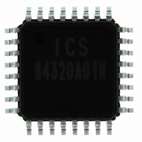
ICS84320AY-01LN IDT, Integrated Device Technology Inc, ICS84320AY-01LN Datasheet - Page 2

ICS84320AY-01LN
Manufacturer Part Number
ICS84320AY-01LN
Description
IC SYNTHESIZER GP LVPECL 32-LQFP
Manufacturer
IDT, Integrated Device Technology Inc
Series
HiPerClockS™r
Type
Frequency Synthesizerr
Datasheet
1.ICS84320AY-01LN.pdf
(22 pages)
Specifications of ICS84320AY-01LN
Pll
Yes with Bypass
Input
Crystal
Output
LVPECL
Number Of Circuits
1
Ratio - Input:output
1:2
Differential - Input:output
No/Yes
Frequency - Max
780MHz
Divider/multiplier
Yes/No
Voltage - Supply
3.135 V ~ 3.465 V
Operating Temperature
0°C ~ 70°C
Mounting Type
Surface Mount
Package / Case
32-LQFP
Frequency-max
780MHz
Number Of Elements
1
Supply Current
155mA
Pll Input Freq (min)
14MHz
Pll Input Freq (max)
40MHz
Operating Supply Voltage (typ)
3.3V
Operating Temp Range
0C to 70C
Package Type
TQFP
Output Frequency Range
77.5 to 780MHz
Operating Supply Voltage (min)
2.915/3.135V
Operating Supply Voltage (max)
3.465V
Operating Temperature Classification
Commercial
Pin Count
32
Lead Free Status / RoHS Status
Lead free / RoHS Compliant
Other names
800-1140
84320AY-01LN
84320AY-01LN
Available stocks
Company
Part Number
Manufacturer
Quantity
Price
Company:
Part Number:
ICS84320AY-01LN
Manufacturer:
IDT, Integrated Device Technology Inc
Quantity:
10 000
Part Number:
ICS84320AY-01LN
Manufacturer:
ICS
Quantity:
20 000
Company:
Part Number:
ICS84320AY-01LNT
Manufacturer:
IDT, Integrated Device Technology Inc
Quantity:
10 000
F
NOTE: The functional description that follows describes op-
eration using a 25MHz crystal. Valid PLL loop divider values
for different crystal or input frequencies are defined in the In-
put Frequency Characteristics, Table 5, NOTE 1.
The ICS84320-01 features a fully integrated PLL and there-
fore requires no external components for setting the loop band-
width. A fundamental crystal is used as the input to the on-
chip oscillator. The output of the oscillator is fed into the phase
detector. A 25MHz crystal provides a 25MHz phase detector
reference frequency. The VCO of the PLL operates over a
range of 620MHz to 780MHz. The output of the M divider is
also applied to the phase detector.
The phase detector and the M divider force the VCO output fre-
quency to be M times the reference frequency by adjusting the
VCO control voltage. Note that for some values of M (either too
high or too low), the PLL will not achieve lock. The output of the
VCO is scaled by a divider prior to being sent to each of the LVPECL
output buffers. The divider provides a 50% output duty cycle.
The programmable features of the ICS84320-01 support two
input modes to program the M divider and N output divider. The
two input operational modes are parallel and serial. Figure 1 shows
the timing diagram for each mode. In parallel mode, the nP_LOAD
input is initially LOW. The data on inputs M0 through M8 and N0
and N1 is passed directly to the M divider and N output divider.
On the LOW-to-HIGH transition of the nP_LOAD input, the data
is latched and the M divider remains loaded until the next
LOW transition on nP_LOAD or until a serial event occurs. As a
result, the M and N bits can be hardwired to set the M divider
and N output divider to a specific default state that will auto-
M0:M8, N0:N1
*NOTE: The NULL timing slot must be observed.
84320AY-01
UNCTIONAL
S_CLOCK
nP_LOAD
nP_LOAD
S_LOAD
S_DATA
S_LOAD
D
ESCRIPTION
t
S
T 1
F
t
IGURE
H
T0
1. P
*NULL
t
M, N
S
ARALLEL
N1
t
H
www.idt.com
Time
P
N0
& S
S
ARALLEL
ERIAL
2
ERIAL
matically occur during power-up. The TEST output is LOW when
operating in the parallel input mode. The relation-ship between
the VCO frequency, the crystal frequency and the M divider is
defined as follows:
The M value and the required values of M0 through M8 are
shown in Table 3B to program the VCO Frequency Function
Table. Valid M values for which the PLL will achieve lock for a
25MHz reference are defined as 25 ≤ M ≤ 31. The frequency
out is defined as follows:
Serial operation occurs when nP_LOAD is HIGH and S_LOAD
is LOW. The shift register is loaded by sampling the S_DATA
bits with the rising edge of S_CLOCK. The contents of the
shift register are loaded into the M divider and N output di-
vider when S_LOAD transitions from LOW-to-HIGH. The M
divide and N output divide values are latched on the HIGH-to-
LOW transition of S_LOAD. If S_LOAD is held HIGH, data at
the S_DATA input is passed directly to the M divider and N
output divider on each rising edge of S_CLOCK. The serial
mode can be used to program the M and N bits and test bits
T1 and T0. The internal registers T0 and T1 determine the state
of the TEST output as follows:
M8
780MH
L
OADING
L
L
M7
OAD
OADING
T1
0
0
1
1
M6
O
LVPECL F
Z
PERATIONS
T0
0
1
0
1
, C
M5
FOUT = fVCO = fxtal x M
RYSTAL
fVCO = fxtal x M
M4
S_Data, Shift Register Input
N
M3
REQUENCY
-
Output of M divider
TO
TEST Output
CMOS Fout
-3.3V D
ICS84320-01
M2
LOW
M1
N
S
M 0
IFFERENTIAL
YNTHESIZER
REV. D JULY 26, 2010
t
S


