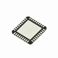
SI5317C-C-GM Silicon Laboratories Inc, SI5317C-C-GM Datasheet - Page 37

SI5317C-C-GM
Manufacturer Part Number
SI5317C-C-GM
Description
IC CLK JITTER CLEANR PROG 36QFN
Manufacturer
Silicon Laboratories Inc
Type
Jitter Cleanerr
Series
Si5317r
Datasheet
1.SI5317C-C-GM.pdf
(46 pages)
Specifications of SI5317C-C-GM
Package / Case
36-QFN
Pll
Yes with Bypass
Input
Clock, Crystal
Output
CML, CMOS, LVDS, LVPECL
Number Of Circuits
1
Ratio - Input:output
1:2
Differential - Input:output
Yes/Yes
Frequency - Max
200MHz
Divider/multiplier
No/No
Voltage - Supply
1.71 V ~ 3.63 V
Operating Temperature
-40°C ~ 85°C
Mounting Type
Surface Mount
Frequency-max
200MHz
Termination Style
SMD/SMT
Load Capacitance
15 pF
Output Format
CMOS
Dimensions
5 mm W x 7 mm L x 1.85 mm H
Minimum Operating Temperature
- 40 C
Maximum Operating Temperature
+ 85 C
Mounting Style
SMD/SMT
Product
XO
Frequency
10 MHz to 160 MHz
Frequency Stability
+/- 20 PPM
Supply Voltage
3.3 Volts
Height
1.85 mm
Lead Free Status / RoHS Status
Lead free / RoHS Compliant
Lead Free Status / RoHS Status
Lead free / RoHS Compliant, Lead free / RoHS Compliant
Other names
336-1921
Available stocks
Company
Part Number
Manufacturer
Quantity
Price
Company:
Part Number:
SI5317C-C-GM
Manufacturer:
SIS
Quantity:
272
Pin #
8,31
15
14
16
17
18
19
20
11
7
6
Pin Name
DBL2_BY
RATE0
RATE1
CKIN+
CKIN–
GND
DEC
LOL
INC
XB
XA
Table 14. Si5317 Pin Descriptions (Continued)
GND
I/O
O
I
I
I
I
I
I
Signal Level
LVCMOS
LVCMOS
LVCMOS
3-Level
3-Level
Analog
Supply
Multi
Note: See Table 13 for settings.
Output 2 Disable/Bypass Mode Control.
Controls enable of CKOUT2 divider/output buffer path and
PLL bypass mode.
L = CKOUT2 enabled
M = CKOUT2 disabled
H = Bypass mode with CKOUT2 enabled
This pin has a weak pull-up and weak pull-down and defaults
to M.
Some designs may require an external resistor voltage
divider when driven by an active device that will tri-state.
Bypass mode is not supported for CMOS clock outputs.
Clock Input.
Differential input clock. This input can also be driven with a
single-ended signal. Input frequency selected from Table 9
on page 22.
PLL Loss of Lock Indicator.
This pin functions as the active high PLL loss of lock indica-
tor.
0 = PLL locked
1 = PLL unlocked
Skew Decrement.
This edge-triggered pin decreases the input to output device
skew. There is no limit on the range of skew adjustment by
this method. Detailed operations and timing characteristics
for this pin are found in Section 3.2, Table 8.
This pin has a weak pull-down.
Skew Increment.
This edge-triggered pin increases the input to output device
skew. There is no limit on the range of skew adjustment by
this method. Detailed operations and timing characteristics
for this pin are found in Section 3.2, Table 8.
This pin has a weak pull-down.
External Crystal or Reference Clock.
External crystal should be connected to these pins to use
internal oscillator-based reference. Crystal or reference clock
selection is set by the XTAL/CLOCK pin. See “AN591:
Crystal Selection for the Si5315 and Si5317.”
Ground.
Must be connected to system ground. Minimize the ground
path impedance for optimal performance of this device.
External Crystal or Reference Clock Rate.
Rev. 1.1
Description
Si5317
37


