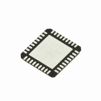
SI5317C-C-GM Silicon Laboratories Inc, SI5317C-C-GM Datasheet - Page 5

SI5317C-C-GM
Manufacturer Part Number
SI5317C-C-GM
Description
IC CLK JITTER CLEANR PROG 36QFN
Manufacturer
Silicon Laboratories Inc
Type
Jitter Cleanerr
Series
Si5317r
Datasheet
1.SI5317C-C-GM.pdf
(46 pages)
Specifications of SI5317C-C-GM
Package / Case
36-QFN
Pll
Yes with Bypass
Input
Clock, Crystal
Output
CML, CMOS, LVDS, LVPECL
Number Of Circuits
1
Ratio - Input:output
1:2
Differential - Input:output
Yes/Yes
Frequency - Max
200MHz
Divider/multiplier
No/No
Voltage - Supply
1.71 V ~ 3.63 V
Operating Temperature
-40°C ~ 85°C
Mounting Type
Surface Mount
Frequency-max
200MHz
Termination Style
SMD/SMT
Load Capacitance
15 pF
Output Format
CMOS
Dimensions
5 mm W x 7 mm L x 1.85 mm H
Minimum Operating Temperature
- 40 C
Maximum Operating Temperature
+ 85 C
Mounting Style
SMD/SMT
Product
XO
Frequency
10 MHz to 160 MHz
Frequency Stability
+/- 20 PPM
Supply Voltage
3.3 Volts
Height
1.85 mm
Lead Free Status / RoHS Status
Lead free / RoHS Compliant
Lead Free Status / RoHS Status
Lead free / RoHS Compliant, Lead free / RoHS Compliant
Other names
336-1921
Available stocks
Company
Part Number
Manufacturer
Quantity
Price
Company:
Part Number:
SI5317C-C-GM
Manufacturer:
SIS
Quantity:
272
Table 2. DC Characteristics (Continued)
(V
Differential Input
Voltage Swing
CKOUT Output Clock
Common Mode
Differential Output Swing
Single-ended Output Swing
Differential Output Voltage
Common Mode
Output Voltage
Differential
Output Voltage
Common Mode
Output Voltage
Output Voltage Low
Output Voltage High
Output Drive Current
2-Level LVCMOS Input Pins
Input Voltage Low
Notes:
DD
1. LVPECL outputs require VDD > 2.25 V.
2. This is the amount of leakage that the 3L inputs can tolerate from an external driver. See Figure 3 on page 9. In most
3. No overshoot or undershoot.
= 1.8 ±5%, 2.5 ±10%, or 3.3 V ±10%, T
designs, an external resistor voltage divider is recommended.
Parameter
1
CKO
CKO
CKO
CKO
Symbol
CKO
CKO
CKO
V
V
V
V
V
OCM
OD
VOHLH
SE
VOLLH
ID
IL
VCM
VCM
VD
VD
IO
A
= –40 to 85 ºC)
put low or CKO
high. CKOUT+ and CKOUT–
Low swing LVDS 100 load
Driving into CKO
LVPECL 100 load
LVPECL 100 load
LVPECL 100 load
f
f
shorted externally.
LVDS 100 load
LVDS 100 load
CKIN
CKIN
CML 100 load
CML 100 load
Test Condition
See Figure 2.
See Figure 2.
V
V
V
V
V
V
Rev. 1.1
line-to-line
line-to-line
line-to-line
line-to-line
line-to-line
line-to-line
line-to-line
line-to-line
DD
DD
DD
DD
DD
DD
< 212.5 MHz
> 212.5 MHz
CMOS
CMOS
CMOS
= 1.71 V
= 1.71 V
= 2.25 V
= 2.97 V
= 1.8 V
= 3.3 V
VOH
VOL
for output
for out-
0.8 x V
V
1.125
0.25
Min
1.42
350
500
350
0.2
1.1
0.5
DD
—
—
—
—
—
—
—
–
DD
V
0.36
Typ
425
700
425
DD
1.2
7.5
32
—
—
—
—
—
—
—
—
—
—
–
V
1.275
Max
0.93
1.25
500
900
500
DD
1.9
0.4
0.5
0.7
0.8
—
—
—
—
—
—
Si5317
–
mV
mV
mV
Units
V
V
V
V
mA
mA
V
V
V
V
V
V
V
V
PP
PP
PP
PP
PP
PP
PP
5


