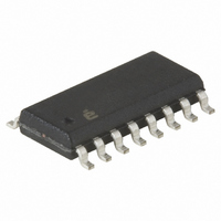
EL4584CSZ Intersil, EL4584CSZ Datasheet - Page 7

EL4584CSZ
Manufacturer Part Number
EL4584CSZ
Description
IC PLL VIDEO GP 36MHZ 16-SOIC
Manufacturer
Intersil
Type
Phase Lock Loop (PLL)r
Datasheet
1.EL4584CSZ.pdf
(15 pages)
Specifications of EL4584CSZ
Pll
Yes
Input
Clock
Output
CMOS, TTL
Number Of Circuits
1
Ratio - Input:output
3:1
Differential - Input:output
No/No
Frequency - Max
36MHz
Divider/multiplier
Yes/No
Voltage - Supply
5V
Operating Temperature
-40°C ~ 85°C
Mounting Type
Surface Mount
Package / Case
16-SOIC (3.9mm Width)
Frequency-max
36MHz
Pll Type
Clock Generation
Frequency
36MHz
Supply Current
2mA
Supply Voltage Range
5V
Digital Ic Case Style
SOIC
No. Of Pins
16
Operating Temperature Range
-40°C To +85°C
Bandwidth
36MHz
Rohs Compliant
Yes
Lead Free Status / RoHS Status
Lead free / RoHS Compliant
Available stocks
Company
Part Number
Manufacturer
Quantity
Price
Company:
Part Number:
EL4584CSZ
Manufacturer:
Intersil
Quantity:
7
Company:
Part Number:
EL4584CSZ-T7
Manufacturer:
ROHM
Quantity:
2 375
Part Number:
EL4584CSZ-T7
Manufacturer:
EVERLIG
Quantity:
20 000
Typical Performance Curves
Block Diagram
Description Of Operation
The horizontal sync signal (CMOS level, falling leading
edge) is input to H
about 200ns, the falling edge of which becomes the
reference to which the clock output will be locked (see
“Timing Diagrams” on page 5 and page 6). The clock is
generated by the signal on pin 5, OSC IN. There are 2
general types of VCO that can be used with the EL4584; LC
and crystal controlled. Additionally, each type can be either
built-up using discrete components, including a varactor as
the frequency controlling element, or complete, self
contained modules can be purchased with everything inside
a metal can. The modules are very forgiving of PCB layout,
but cost more than discrete solutions. The VCO or VCXO is
used to generate the clock. An LC tank resonator has
greater “pull” than a crystal controlled circuit, but will also be
more likely to drift over time, and thus will generate more
jitter. The “pullability” of the circuit refers to the ability to “pull”
the frequency of oscillation away from its center frequency
by modulating the voltage on the control pin of a VCO
module or varactor, and is a function of the slope and range
SYNC
input (pin 10). This signal is delayed
FIGURE 10. PACKAGE POWER DISSIPATION VS AMBIENT TEMPERATURE
7
(Continued)
2.0
1.8
1.6
1.4
1.2
1.0
0.8
0.6
0.4
0.2
0
0
JEDEC JESD51-7 HIGH EFFECTIVE THERMAL
CONDUCTIVITY TEST BOARD
1.43W
1.25W
θ
SO16 (0.150”)
JA
AMBIENT TEMPERATURE (°C)
25
= +80°C/W
EL4584
50
θ
JA
PDIP16
= +70°C/W
75
of the capacitance-voltage curve of the varactor or VCO
module used. The VCO signal is sent to a divide by N
counter, and to the CLK OUT pin. The divisor N is
determined by the state of pins 1, 2 and 16 and is described
in Table 2. The divided signal is sent, along with the delayed
H
compares the two signals for phase and frequency
differences. Any phase difference is converted to a current at
the charge pump output FILTER (pin 7). A VCO with positive
frequency deviation with control voltage must be used.
Varactors have negative capacitance slope with voltage,
resulting in positive frequency deviation with control voltage
for the oscillators in Figures 12 and 13.
VCO
The VCO should be tuned so its frequency of oscillation is
very close to the required clock output frequency when the
voltage on the varactor is 2.5V. VCXO and VCO modules are
already tuned to the desired frequency, so this step is not
necessary if using one of these units. The range of the
charge pump output (pin 7) is 0V to 5V and it can source or
sink a maximum of about 300µA, so all frequency control
SYNC
100
input, to the phase/frequency detector, which
125
150
May 9, 2008
FN7174.3


