LMX2434TMX/NOPB National Semiconductor, LMX2434TMX/NOPB Datasheet
LMX2434TMX/NOPB
Specifications of LMX2434TMX/NOPB


Related parts for LMX2434TMX/NOPB


LMX2434TMX/NOPB Summary of contents
Page 1
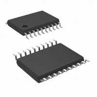
... The LMX243x devices are available in 20-Pin TSSOP and 20-Pin UTCSP surface mount plastic packages. Thin Shrink Small Outline Package (MTC20) PLLatinum ™ trademark of National Semiconductor Corporation. © 2003 National Semiconductor Corporation Features n Low Current Consumption n 2.25V to 2.75V Operation n Selectable Synchronous or Asynchronous Powerdown ...
Page 2
Functional Block Diagram Note: 1 (2) refers to Pin # 1 of the 20-Pin UTCSP and Pin # 2 of the 20-Pin TSSOP www.national.com 2 20053501 ...
Page 3
Connection Diagrams Ultra Thin Chip Scale Package (SLE) (Top View) Pin Descriptions Pin No. Pin No. Pin Name UTCSP TSSOP 1 2 GND 2 3 FinIF CPoutIF 5 6 ENosc 6 7 OSCout/ FLoutIF 7 ...
Page 4
Pin Descriptions (Continued) Pin No. Pin No. Pin Name UTCSP TSSOP 10 11 FLoutRF 11 12 GND 12 13 CPoutRF 13 14 GND 14 15 FinRF 15 16 FinRF * 16 17 Vcc CLK 19 ...
Page 5
Ordering Information Model Temperature Range LMX2430TM -40˚C to +85˚C LMX2430TMX -40˚C to +85˚C LMX2430SLEX -40˚C to +85˚C LMX2433TM -40˚C to +85˚C LMX2433TMX -40˚C to +85˚C LMX2433SLEX -40˚C to +85˚C LMX2434TM -40˚C to +85˚C LMX2434TMX -40˚C to +85˚C LMX2434SLEX -40˚C to ...
Page 6
... Absolute Maximum Ratings Military/Aerospace specified devices are required, please contact the National Semiconductor Sales Office/ Distributors for availability and specifications. Power Supply Voltage Vcc to GND Voltage on any pin to GND ( < V must be +3.25V I Storage Temperature Range ( Lead Temperature (solder Electrical Characteristics Vcc = EN = 2.5V, −40˚C ≤ T ≤ ...
Page 7
Electrical Characteristics Vcc = EN = 2.5V, −40˚C ≤ T ≤ +85˚C, unless otherwise specified A Symbol Parameter RF SYNTHESIZER PARAMETERS I RF Charge Pump Output Source CPoutRF Source Current I RF Charge Pump Output Sink Current V CPoutRF Sink ...
Page 8
Electrical Characteristics Vcc = EN = 2.5V, −40˚C ≤ T ≤ +85˚C, unless otherwise specified A Symbol Parameter IF SYNTHESIZER PARAMETERS I IF Charge Pump Output TRI-STATE CPoutIF TRI Current I IF Charge Pump Output Sink Current CPoutIF %MIS Vs ...
Page 9
Electrical Characteristics Vcc = EN = 2.5V, −40˚C ≤ T ≤ +85˚C, unless otherwise specified A Symbol Parameter PHASE NOISE CHARACTERISTICS L (f) RF Synthesizer Normalized Phase NRF Noise Contribution (Note 10) L (f) IF Synthesizer Normalized Phase NIF Noise ...
Page 10
Charge Pump Current Specification Definitions = Vcc − ∆ Charge Pump Sink Current at V CPout I2 = Charge Pump Sink Current Vcc//2 CPout = ∆ Charge Pump Sink Current at V CPout ...
Page 11
Typical Performance Characteristics Sensitivity LMX2430 FinRF Input Power Vs Frequency Vcc = EN = 2.25V LMX2430 FinRF Input Power Vs Frequency Vcc = EN = 2.75V 11 20053592 20053593 www.national.com ...
Page 12
Typical Performance Characteristics Sensitivity (Continued) www.national.com LMX2433 FinRF Input Power Vs Frequency Vcc = EN = 2.25V LMX2433 FinRF Input Power Vs Frequency Vcc = EN = 2.75V 12 20053594 20053595 ...
Page 13
Typical Performance Characteristics Sensitivity (Continued) LMX2434 FinRF Input Power Vs Frequency Vcc = EN = 2.35V LMX2434 FinRF Input Power Vs Frequency Vcc = EN = 2.75V 13 20053596 20053597 www.national.com ...
Page 14
Typical Performance Characteristics Sensitivity (Continued) www.national.com LMX2430 FinIF Input Power Vs Frequency Vcc = EN = 2.25V LMX2430 FinIF Input Power Vs Frequency Vcc = EN = 2.75V 14 20053598 20053599 ...
Page 15
Typical Performance Characteristics Sensitivity (Continued) LMX2433 FinIF Input Power Vs Frequency Vcc = EN = 2.25V LMX2433 FinIF Input Power Vs Frequency Vcc = EN = 2.75V 15 200535A0 200535A1 www.national.com ...
Page 16
Typical Performance Characteristics Sensitivity (Continued) www.national.com LMX2434 FinIF Input Power Vs Frequency Vcc = EN = 2.25V LMX2434 FinIF Input Power Vs Frequency Vcc = EN = 2.75V 16 200535A2 200535A3 ...
Page 17
Typical Performance Characteristics Sensitivity (Continued) LMX243x OSCin Input Voltage Vs Frequency Vcc = EN = 2.25V LMX243x OSCin Input Voltage Vs Frequency Vcc = EN = 2.75V 17 200535A4 200535A5 www.national.com ...
Page 18
Typical Performance Characteristics Charge Pump www.national.com LMX243x RF Charge Pump Sweeps Vcc = EN = 2.50V −40˚C ≤ T ≤ +85˚C A LMX243x IF Charge Pump Sweeps Vcc = EN = 2.50V −40˚C ≤ T ≤ +85˚ 200535A6 ...
Page 19
Typical Performance Characteristics Input Impedance LMX243x UTCSP FinRF Input Impedance Vcc = EN = 2.50V +25˚C A LMX243x UTCSP FinIF Input Impedance Vcc = EN = 2.50V +25˚C A LMX243x TSSOP FinRF Input Impedance Vcc = ...
Page 20
Typical Performance Characteristics Input Impedance (Continued) LMX243x UTCSP OSCin Input Impedance Vs Frequency LMX233xU TSSOP OSCin Input Impedance Vs Frequency www.national.com Vcc = EN = 2.50V T = +25˚C A Vcc = EN = 2.50V T = +25˚ ...
Page 21
LMX243x UTCSP FinRF Input Impedance Table Vcc = EN = 2.50V +25˚ |Γ| FinRF (MHz) 100 0.86 200 0.86 300 0.85 400 0.84 500 0.83 600 0.82 700 0.82 800 0.81 900 0.80 1000 0.80 1100 ...
Page 22
LMX243x UTCSP FinRF Input Impedance Table Vcc = EN = 2.50V +25˚ |Γ| FinRF (MHz) 4900 0.84 5000 0.84 5100 0.84 5200 0.84 5300 0.84 5400 0.84 5500 0.83 5600 0.83 5700 0.82 5800 0.82 5900 ...
Page 23
LMX243x TSSOP FinRF Input Impedance Table Vcc = EN = 2.50V +25˚ |Γ| FinRF (MHz) 100 0.86 200 0.85 300 0.84 400 0.83 500 0.82 600 0.82 700 0.82 800 0.82 900 0.81 1000 0.80 1100 ...
Page 24
LMX243x TSSOP FinRF Input Impedance Table Vcc = EN = 2.50V +25˚ |Γ| FinRF (MHz) 4900 0.75 5000 0.75 5100 0.76 5200 0.77 5300 0.78 5400 0.78 5500 0.76 5600 0.73 5700 0.71 5800 0.68 5900 ...
Page 25
LMX243x UTCSP FinIF Input Impedance Table Vcc = EN = 2.50V +25˚ |Γ| FinIF (MHz) 100 0.87 200 0.86 300 0.85 400 0.84 500 0.83 600 0.83 700 0.82 800 0.81 900 0.80 1000 0.79 1100 ...
Page 26
LMX243x TSSOP FinIF Input Impedance Table Vcc = EN = 2.50V +25˚ |Γ| FinIF (MHz) 100 0.87 200 0.86 300 0.85 400 0.84 500 0.84 600 0.83 700 0.83 800 0.82 900 0.81 1000 0.80 1100 ...
Page 27
LMX243x UTCSP OSCin Input Impedance Table Vcc = EN = 2.50V +25˚ OSCin (MHz) Re {ZOSCin} Im {ZOSCin} (Ω) 5.0 5032.01 7.5 2529.17 10.0 1412.10 12.5 1051.18 15.0 710.63 17.5 545.87 20.0 442.32 22.5 314.15 25.0 ...
Page 28
LMX243x TSSOP OSCin Input Impedance Table Vcc = EN = 2.50V +25˚ OSCin (MHz) Re {ZOSCin} (Ω) 5.0 1111.30 7.5 628.81 10.0 359.99 12.5 284.12 15.0 203.53 17.5 134.32 20.0 109.85 22.5 80.56 25.0 69.37 27.5 ...
Page 29
LMX243x Charge Pump Test Setup The block diagram above illustrates the setup required to measure the LMX243x device’s RF charge pump sink cur- rent. The same setup is used for the LMX2430TM Evaluation Board. The purpose of this test is ...
Page 30
LMX243x FinRF Sensitivity Test Setup The block diagram above illustrates the setup required to measure the LMX243x device’s RF input sensitivity level. The same setup is used for the LMX2430TM Evaluation Board. The purpose of this test is to measure ...
Page 31
LMX243x OSCin Sensitivity Test Setup The block diagram above illustrates the setup required to measure the LMX243x device’s OSCin buffer sensitivity level. The same setup is used for the LMX2430TM Evalua- tion Board. This setup is similar to the FinRF ...
Page 32
LMX243x FinRF Input Impedance Test Setup The block diagram above illustrates the setup required to measure the LMX243x device’s RF input impedance. The same setup is used for the LMX2430TM Evaluation Board. Measuring the device’s input impedance facilitates the de- ...
Page 33
LMX243x Serial Data Input Timing Notes: 1. DATA is clocked into the 24-bit shift register on the rising edge of CLK 2. The MSB of DATA is shifted in first. 33 20053510 www.national.com ...
Page 34
... Functional Description The basic phase-lock-loop (PLL) configuration consists of a high-stability crystal reference oscillator, a frequency synthe- sizer such as the National Semiconductor LMX243x, a volt- age controlled oscillator (VCO), and a passive loop filter. The frequency synthesizer includes a phase detector, current mode charge pump, programmable reference R and feed- back N frequency dividers ...
Page 35
Functional Description 1.5.1 Phase Comparator and Internal Charge Pump Characteristics Notes: 1. The minimum width of the pump-up and pump-down current pulses occur at the CPoutRF or CPoutIF pins when the loop is phase locked. 2. The diagram assumes ...
Page 36
Functional Description 1.8.3 Digital Filtered Lock Detect Output A digital filtered lock detect status generated from the phase detector is also available on the Ftest/LD output pin if se- lected. The lock detect digital filter compares the difference bewteen ...
Page 37
Functional Description 1.8.4 Reference Divider and Feedback Divider Output The outputs of the various N and R dividers can be moni- tored by selecting the appropriate Ftest/LD word. This is essential when performing OSCin or Fin sensitivity measure- ments. ...
Page 38
Programming Description 2.1 MICROWIRE INTERFACE The 24-bit shift register is loaded via the MICROWIRE interface. The shift register consists of a 21-bit DATA[20:0] FIELD and a 3-bit ADDRESS[2:0] FIELD as shown below. The ADDRESS FIELD is used to decode ...
Page 39
Programming Description 2.4 R0 REGISTER The R0 register contains the RF_R, RF_CPP, RF_CPG, RF_CPT, and RF_RST control words, in addition to two of the four bits that compose the MUX control word. The detailed descriptions and programming information for ...
Page 40
Programming Description 2.4.3 RF_CPG - RF Synthesizer Charge Pump Current Gain (R0[19]) The RF_CPG bit controls the RF synthesizer’s charge pump gain. Two gain levels are available. Control Bit Register Location RF_CPG 2.4.4 RF_CPT - RF Synthesizer Charge Pump ...
Page 41
Programming Description 2.5.1.2 RF_A[4:0] - LMX2434 RF Synthesizer Swallow Counter (A Counter) (R1[7:3]) The LMX2434 A counter is a 5-bit swallow counter used in the programmable feedback divider. The RF_A control word can be programmed to values ranging from ...
Page 42
Programming Description 2.5.4 RF_PD - RF Synthesizer Powerdown (R1[23]) The RF_PD bit is used to switch the RF PLL between a powered up and powered down mode. Furthermore, the RF_PD bit operates in conjuction with the RF_CPT bit to ...
Page 43
Programming Description 2.7 R3 REGISTER The R3 register contains the IF_R, IF_CPP, IF_CPG, IF_CPT, and IF_RST control words, in addition to two of the four bits that compose the MUX control word. The detailed descriptions and programming information for ...
Page 44
Programming Description 2.7.3 IF_CPG - IF Synthesizer Charge Pump Current Gain (R3[19]) The IF_CPG bit controls the IF synthesizer’s charge pump gain. Two gain levels are available. Control Bit Register Location IF_CPG 2.7.4 IF_CPT - IF Synthesizer Charge Pump ...
Page 45
Programming Description 2.8.2 IF_B[13: Synthesizer Programmable Binary Counter (B Counter) (R4[20:7]) The IF_B control word is used to setup the IF synthesizer’s B counter. The B counter is a 14-bit programmable binary counter used in the programmable ...
Page 46
Programming Description 2.9 R5 REGISTER The R5 Register contains the IF_TOC control word. The IF_TOC is used to setup the IF syhnthesizer’s Fastlock circuitry. The IF_TOC is a 12-bit binary counter programmable from 0 to 4095. Reg 23 22 ...
Page 47
Programming Description 2.10 MUX[3:0] - MULTIFUNCTION OUTPUT SELECT (R3[23:22]:R0[23:22]) The MUX control word is used to determine which signal is routed to the Ftest/LD pin. MUX[3: ...
Page 48
Physical Dimensions www.national.com inches (millimeters) unless otherwise noted 20-Pin Ultra Thin Chip Scale Package (UTCSP) NS Package Number SLE20A 48 ...
Page 49
... NATIONAL’S PRODUCTS ARE NOT AUTHORIZED FOR USE AS CRITICAL COMPONENTS IN LIFE SUPPORT DEVICES OR SYSTEMS WITHOUT THE EXPRESS WRITTEN APPROVAL OF THE PRESIDENT AND GENERAL COUNSEL OF NATIONAL SEMICONDUCTOR CORPORATION. As used herein: 1. Life support devices or systems are devices or systems which, (a) are intended for surgical implant ...