LMX2434TMX/NOPB National Semiconductor, LMX2434TMX/NOPB Datasheet - Page 4
LMX2434TMX/NOPB
Manufacturer Part Number
LMX2434TMX/NOPB
Description
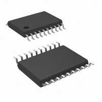
IC SYNTHESIZER DUAL 5GHZ 20TSSOP
Manufacturer
National Semiconductor
Series
PLLatinum™r
Type
PLL Frequency Synthesizerr
Datasheet
1.LMX2433SLEXNOPB.pdf
(49 pages)
Specifications of LMX2434TMX/NOPB
Pll
Yes with Bypass
Input
CMOS
Output
CMOS
Number Of Circuits
1
Ratio - Input:output
3:2
Differential - Input:output
Yes/No
Frequency - Max
5GHz, 2.5GHz
Divider/multiplier
No/No
Voltage - Supply
2.25 V ~ 2.75 V
Operating Temperature
-40°C ~ 85°C
Mounting Type
Surface Mount
Package / Case
20-TSSOP
Frequency-max
5GHz
For Use With
LMX2434EVAL - EVALUATION BOARD FOR LMX2434
Lead Free Status / RoHS Status
Lead free / RoHS Compliant
Other names
LMX2434TMX


www.national.com
Pin No.
UTCSP
Pin Descriptions
10
11
12
13
14
15
16
17
18
19
20
Pin No.
TSSOP
11
12
13
14
15
16
17
18
19
20
1
Pin Name
CPoutRF
FLoutRF
FinRF
FinRF
DATA
GND
GND
CLK
Vcc
Vcc
LE
*
(Continued)
I/O
—
—
—
—
O
O
I
I
I
I
I
RF PLL Fastlock output. This pin connects a resistor in parallel to R2 of the
external loop filter. This pin can also function as a general purpose CMOS
TRI-STATE output.
Ground for the RF PLL digital circuits.
RF PLL charge pump output. The output is connected to the external loop filter,
which drives the input of the RF VCO.
Ground for the RF PLL analog circuits.
RF PLL prescaler input. Small signal input from the VCO.
RF PLL prescaler complementary input. For single ended operation, this pin
should be AC grounded through a 100 pF capacitor. The LMX243x can be
driven differentially when the AC coupled capacitor is omitted.
Power supply bias for the RF PLL analog circuits. Vcc may range from 2.25V to
2.75V. Bypass capacitors should be placed as close as possible to this pin and
be connected directly to the ground plane.
MICROWIRE Latch Enable input. High impedance CMOS input. When LE
transitions HIGH, DATA stored in the shift register is loaded into one of 6
internal control registers.
MICROWIRE Clock input. High impedance CMOS input. DATA is clocked into
the 24-bit shift register on the rising edge of CLK.
MICROWIRE Data input. High impedance CMOS input. Binary serial data. The
MSB of DATA is shifted in first. The two last bits are the control bits.
Power supply bias for the IF PLL analog and digital circuits, MICROWIRE, and
Ftest/LD circuits. Vcc may range from 2.25V to 2.75V. Bypass capacitors
should be placed as close as possible to this pin and be connected directly to
the ground plane
4
Description
Related parts for LMX2434TMX/NOPB
Image
Part Number
Description
Manufacturer
Datasheet
Request
R

Part Number:
Description:
IC FREQ SYNTH DUAL 20TSSOP
Manufacturer:
National Semiconductor
Datasheet:

Part Number:
Description:
National Semiconductor [8-Bit D/A Converter]
Manufacturer:
National Semiconductor
Datasheet:
Part Number:
Description:
National Semiconductor [Media Coprocessor]
Manufacturer:
National Semiconductor
Datasheet:
Part Number:
Description:
Digitally Controlled Tone and Volume Circuit with Stereo Audio Power Amplifier, Microphone Preamp Stage and National 3D Sound
Manufacturer:
National Semiconductor
Datasheet:
Part Number:
Description:
Digitally Controlled Tone and Volume Circuit with Stereo Audio Power Amplifier, Microphone Preamp Stage and National 3D Sound
Manufacturer:
National Semiconductor
Datasheet:
Part Number:
Description:
AC97 Rev 2 Codec with Sample Rate Conversion and National 3D Sound
Manufacturer:
National Semiconductor
Part Number:
Description:
Manufacturer:
National Semiconductor
Datasheet:
Part Number:
Description:
Manufacturer:
National Semiconductor
Datasheet:
Part Number:
Description:
General Purpose, Low Voltage, Low Power, Rail-to-Rail Output Operational Amplifiers
Manufacturer:
National Semiconductor
Datasheet:
Part Number:
Description:
8-bit 20 MSPS flash A/D converter.
Manufacturer:
National Semiconductor
Datasheet:
Part Number:
Description:
Low Noise Quad Operational Amplifier
Manufacturer:
National Semiconductor
Datasheet:
Part Number:
Description:
Quad Differential Line Receivers
Manufacturer:
National Semiconductor
Datasheet:
Part Number:
Description:
Quad High Speed Trapezoidal? Bus Transceiver
Manufacturer:
National Semiconductor
Datasheet:
Part Number:
Description:
Dual Line Receiver
Manufacturer:
National Semiconductor
Datasheet: