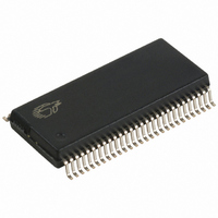
CY28411OXC-1 Cypress Semiconductor Corp, CY28411OXC-1 Datasheet - Page 4

CY28411OXC-1
Manufacturer Part Number
CY28411OXC-1
Description
IC CLOCK GEN ALVISO 56-SSOP
Manufacturer
Cypress Semiconductor Corp
Type
Fanout Distribution, Spread Spectrum Clock Generatorr
Datasheet
1.CY28411OXC-1.pdf
(19 pages)
Specifications of CY28411OXC-1
Pll
Yes
Input
LVTTL, Crystal
Output
Clock
Number Of Circuits
1
Ratio - Input:output
7:20
Differential - Input:output
No/Yes
Frequency - Max
266MHz
Divider/multiplier
Yes/No
Voltage - Supply
3.135 V ~ 3.465 V
Operating Temperature
0°C ~ 85°C
Mounting Type
Surface Mount
Package / Case
56-SSOP
Frequency-max
100MHz
Lead Free Status / RoHS Status
Lead free / RoHS Compliant
Document #: 38-07694 Rev. *B
Table 3. Block Read and Block Write Protocol (continued)
Table 4. Byte Read and Byte Write Protocol
Control Registers
Byte 0:Control Register 0
36:29
45:38
18:11
27:20
Bit
8:2
Bit
Bit
28
37
46
....
....
....
....
10
19
28
29
1
9
7
6
5
4
3
Acknowledge from slave
Data byte 1 – 8 bits
Acknowledge from slave
Data byte 2 – 8 bits
Acknowledge from slave
Data Byte /Slave Acknowledges
Data Byte N –8 bits
Acknowledge from slave
Stop
Start
Slave address – 7 bits
Write
Acknowledge from slave
Command Code – 8 bits
Acknowledge from slave
Data byte – 8 bits
Acknowledge from slave
Stop
@Pup
1
1
1
1
1
Block Write Protocol
Byte Write Protocol
CPUC2_ITP/SRCC7
CPUT2_ITP/SRCT7
Description
Description
SRC[T/C]6
SRC[T/C]5
SRC[T/C]4
SRC[T/C]3
Name
CPU[T/C]2_ITP/SRC[T/C]7 Output Enable
0 = Disable (Hi-Z), 1 = Enable
SRC[T/C]6 Output Enable
0 = Disable (Hi-Z), 1 = Enable
SRC[T/C]5 Output Enable
0 = Disable (Hi-Z), 1 = Enable
SRC[T/C]4 Output Enable
0 = Disable (Hi-Z), 1 = Enable
SRC[T/C]3 Output Enable
0 = Disable (Hi-Z), 1 = Enable
27:21
37:30
46:39
55:48
27:21
37:30
18:11
Bit
28
29
38
47
56
....
....
....
....
8:2
Bit
10
19
20
28
29
38
39
1
9
Slave address – 7 bits
Read = 1
Acknowledge from slave
Byte Count from slave – 8 bits
Acknowledge
Data byte 1 from slave – 8 bits
Acknowledge
Data byte 2 from slave – 8 bits
Acknowledge
Data bytes from slave / Acknowledge
Data Byte N from slave – 8 bits
NOT Acknowledge
Stop
Start
Slave address – 7 bits
Write
Acknowledge from slave
Command Code – 8 bits
Acknowledge from slave
Repeated start
Slave address – 7 bits
Read
Acknowledge from slave
Data from slave – 8 bits
NOT Acknowledge
Stop
Description
Block Read Protocol
Byte Read Protocol
Description
Description
CY28411-1
Page 4 of 19


