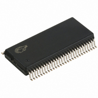
CY28411OXC-1 Cypress Semiconductor Corp, CY28411OXC-1 Datasheet - Page 8

CY28411OXC-1
Manufacturer Part Number
CY28411OXC-1
Description
IC CLOCK GEN ALVISO 56-SSOP
Manufacturer
Cypress Semiconductor Corp
Type
Fanout Distribution, Spread Spectrum Clock Generatorr
Datasheet
1.CY28411OXC-1.pdf
(19 pages)
Specifications of CY28411OXC-1
Pll
Yes
Input
LVTTL, Crystal
Output
Clock
Number Of Circuits
1
Ratio - Input:output
7:20
Differential - Input:output
No/Yes
Frequency - Max
266MHz
Divider/multiplier
Yes/No
Voltage - Supply
3.135 V ~ 3.465 V
Operating Temperature
0°C ~ 85°C
Mounting Type
Surface Mount
Package / Case
56-SSOP
Frequency-max
100MHz
Lead Free Status / RoHS Status
Lead free / RoHS Compliant
Document #: 38-07694 Rev. *B
Calculating Load Capacitors
In addition to the standard external trim capacitors, trace
capacitance and pin capacitance must also be considered to
correctly calculate crystal loading. As mentioned previously,
the capacitance on each side of the crystal is in series with the
As mentioned previously, the capacitance on each side of the
crystal is in series with the crystal. This mean the total capac-
itance on each side of the crystal must be twice the specified
load capacitance (CL). While the capacitance on each side of
the crystal is in series with the crystal, trim capacitors
(Ce1,Ce2) should be calculated to provide equal capacitance
loading on both sides.
Use the following formulas to calculate the trim capacitor
values for Ce1 and Ce2.
CLe
Total Capacitance (as seen by the crystal)
=
(
Load Capacitance (each side)
Ce1 + Cs1 + Ci1
Ce = 2 * CL – (Cs + Ci)
1
+
1
Ce2 + Cs2 + Ci2
Cs1
Figure 1. Crystal Capacitive Clarification
1
Figure 2. Crystal Loading Example
Ce1
X1
Ci1
Clock Chip
)
XTAL
Ci2
crystal. This means the total capacitance on each side of the
crystal must be twice the specified crystal load capacitance
(CL). While the capacitance on each side of the crystal is in
series with the crystal, trim capacitors (Ce1,Ce2) should be
calculated to provide equal capacitive loading on both sides.
CL ....................................................Crystal load capacitance
CLe ......................................... Actual loading seen by crystal
using standard value trim capacitors
Ce ..................................................... External trim capacitors
Cs ..............................................Stray capacitance (terraced)
Ci .......................................................... Internal capacitance
(lead frame, bond wires etc.)
X2
Ce2
Cs2
3 to 6p
33pF
Pin
Trim
Trace
2.8pF
CY28411-1
Page 8 of 19


