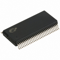
CY28411OXC-1 Cypress Semiconductor Corp, CY28411OXC-1 Datasheet - Page 7

CY28411OXC-1
Manufacturer Part Number
CY28411OXC-1
Description
IC CLOCK GEN ALVISO 56-SSOP
Manufacturer
Cypress Semiconductor Corp
Type
Fanout Distribution, Spread Spectrum Clock Generatorr
Datasheet
1.CY28411OXC-1.pdf
(19 pages)
Specifications of CY28411OXC-1
Pll
Yes
Input
LVTTL, Crystal
Output
Clock
Number Of Circuits
1
Ratio - Input:output
7:20
Differential - Input:output
No/Yes
Frequency - Max
266MHz
Divider/multiplier
Yes/No
Voltage - Supply
3.135 V ~ 3.465 V
Operating Temperature
0°C ~ 85°C
Mounting Type
Surface Mount
Package / Case
56-SSOP
Frequency-max
100MHz
Lead Free Status / RoHS Status
Lead free / RoHS Compliant
Document #: 38-07694 Rev. *B
Byte 6: Control Register 6
Byte 7: Vendor ID
Crystal Recommendations
The CY28411-1 requires a Parallel Resonance Crystal.
Substituting a series resonance crystal will cause the
CY28411-1 to operate at the wrong frequency and violate the
ppm specification. For most applications there is a 300-ppm
frequency shift between series and parallel crystals due to
incorrect loading.
Table 5. Crystal Recommendations
7
6
5
4
3
2
1
0
14.31818 MHz
Frequency
Bit
Bit
1
7
6
5
4
3
2
0
(Fund)
Externally
Externally
Externally
selected
selected
selected
@Pup
@Pup
0
0
0
1
1
0
0
1
0
1
0
0
0
Cut
AT
Revision Code Bit 3
Revision Code Bit 2
Revision Code Bit 1
Revision Code Bit 0
Vendor ID Bit 3
Vendor ID Bit 2
Vendor ID Bit 1
Vendor ID Bit 0
Loading Load Cap
Parallel
PCIF, SRC, PCI
Reserved
CPUT/C
CPUT/C
CPUT/C
Name
Name
REF
20 pF
0.1 mW
REF/N or Hi-Z Select
0 = Hi-Z, 1 = REF/N Clock
Test Clock Mode Entry Control
0 = Normal operation, 1 = REF/N or Hi-Z mode,
Reserved, Set = 0
REF Output Drive Strength
0 = Low, 1 = High
SW PCI_STP Function
0=SW PCI_STP assert, 1= SW PCI_STP deassert
When this bit is set to 0, all STOPPABLE PCI, PCIF and SRC outputs will
be stopped in a synchronous manner with no short pulses.
When this bit is set to 1, all STOPPED PCI, PCIF and SRC outputs will
resume in a synchronous manner with no short pulses.
FS_C Reflects the value of the FS_C pin sampled on power up
0 = FS_C was low during VTT_PWRGD# assertion
FS_B Reflects the value of the FS_B pin sampled on power up
0 = FS_B was low during VTT_PWRGD# assertion
FS_A Reflects the value of the FS_A pin sampled on power up
0 = FS_A was low during VTT_PWRGD# assertion
(max.)
Revision Code Bit 3
Revision Code Bit 2
Revision Code Bit 1
Revision Code Bit 0
Vendor ID Bit 3
Vendor ID Bit 2
Vendor ID Bit 1
Vendor ID Bit 0
Drive
Shunt Cap
Crystal Loading
Crystal loading plays a critical role in achieving low ppm perfor-
mance. To realize low ppm performance, the total capacitance
the crystal will see must be considered to calculate the appro-
priate capacitive loading (CL).
The following diagram shows a typical crystal configuration
using the two trim capacitors. An important clarification for the
following discussion is that the trim capacitors are in series
with the crystal not parallel. It’s a common misconception that
load capacitors are in parallel with the crystal and should be
approximately equal to the load capacitance of the crystal.
This is not true.
(max.)
5 pF
Motional
0.016 pF
(max.)
Description
Description
Tolerance
35 ppm
(max.)
Stability
30 ppm
(max.)
CY28411-1
Page 7 of 19
(max.)
Aging
5 ppm


