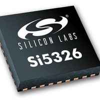
SI5326C-B-GM Silicon Laboratories Inc, SI5326C-B-GM Datasheet - Page 3

SI5326C-B-GM
Manufacturer Part Number
SI5326C-B-GM
Description
IC ANY-RATE MULTI/ATTEN 36QFN
Manufacturer
Silicon Laboratories Inc
Type
Clock Multiplierr
Specifications of SI5326C-B-GM
Number Of Circuits
1
Package / Case
36-QFN
Pll
Yes
Input
Clock
Output
CML, CMOS, LVDS, LVPECL
Ratio - Input:output
2:2
Differential - Input:output
Yes/Yes
Frequency - Max
346MHz
Divider/multiplier
Yes/Yes
Voltage - Supply
1.62 V ~ 3.63 V
Operating Temperature
-40°C ~ 85°C
Mounting Type
Surface Mount
Frequency-max
346MHz
Maximum Input Frequency
710 MHz
Minimum Input Frequency
0.002 MHz
Output Frequency Range
0.002 MHz to 1400 MHz
Supply Voltage (max)
3.63 V
Supply Voltage (min)
1.71 V
Maximum Operating Temperature
+ 85 C
Minimum Operating Temperature
- 40 C
Mounting Style
SMD/SMT
Operating Supply Voltage
1.8 V, 2.5 V, 3.3 V
Lead Free Status / RoHS Status
Lead free / RoHS Compliant
Table 1. Performance Specifications (Continued)
(V
Table 2. Absolute Maximum Ratings
Duty Cycle
PLL Performance
Jitter Generation
Jitter Transfer
External Reference Jitter
Transfer
Phase Noise
Subharmonic Noise
Spurious Noise
Package
Thermal Resistance
Junction to Ambient
Note: For a more comprehensive listing of device specifications, please consult the Silicon Laboratories Any-Rate Precision
DC Supply Voltage
LVCMOS Input Voltage
Operating Junction Temperature
Storage Temperature Range
ESD HBM Tolerance (100 pF, 1.5 kΩ)
ESD MM Tolerance
Latch-Up Tolerance
Note: Permanent device damage may occur if the Absolute Maximum Ratings are exceeded. Functional operation should be
DD
= 1.8, 2.5, or 3.3 V ±10%, T
Clock Family Reference Manual. This document can be downloaded from www.silabs.com/timing.
restricted to the conditions as specified in the operation sections of this data sheet. Exposure to absolute maximum
rating conditions for extended periods of time may affect device reliability.
Parameter
Parameter
Theta JA
Symbol
J
SP
SP
CKO
CKO
A
PKEXTN
J
J
= –40 to 85 ºC)
GEN
SUBH
SPUR
PK
DC
PN
Phase Noise @ 100 kHz Off-
(n > 1, n x F3 < 100 MHz)
LVPECL output format
f
f
Max spur @ n x F3
OUT
OUT
50 kHz–80 MHz
12 kHz–20 MHz
800 Hz–80 MHz
Test Condition
100 kHz offset
Confidential Rev. 0.2
100 Hz offset
10 kHz offset
1 MHz offset
1 kHz offset
= 622.08 MHz,
= 622.08 MHz
Still Air
set
Symbol
T
V
T
V
STG
JCT
DIG
DD
Min
45
—
—
—
—
—
—
—
—
—
—
—
—
—
–0.3 to (V
–0.5 to 3.6
–55 to 150
–55 to 150
JESD78 Compliant
Value
200
TBD
TBD
TBD
TBD
TBD
TBD
TBD
TBD
TBD
0.05
TBD
2
Typ
0.3
0.3
—
DD
+ 0.3)
Max
TBD
TBD
TBD
TBD
TBD
TBD
TBD
TBD
TBD
TBD
TBD
0.1
Si5326
55
—
Unit
kV
ºC
ºC
dBc/Hz
dBc/Hz
dBc/Hz
dBc/Hz
dBc/Hz
ps rms
ps rms
ps rms
V
V
V
ºC/W
Unit
dBc
dBc
dB
dB
%
3


