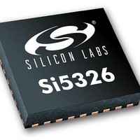
SI5326C-B-GM Silicon Laboratories Inc, SI5326C-B-GM Datasheet - Page 6

SI5326C-B-GM
Manufacturer Part Number
SI5326C-B-GM
Description
IC ANY-RATE MULTI/ATTEN 36QFN
Manufacturer
Silicon Laboratories Inc
Type
Clock Multiplierr
Specifications of SI5326C-B-GM
Number Of Circuits
1
Package / Case
36-QFN
Pll
Yes
Input
Clock
Output
CML, CMOS, LVDS, LVPECL
Ratio - Input:output
2:2
Differential - Input:output
Yes/Yes
Frequency - Max
346MHz
Divider/multiplier
Yes/Yes
Voltage - Supply
1.62 V ~ 3.63 V
Operating Temperature
-40°C ~ 85°C
Mounting Type
Surface Mount
Frequency-max
346MHz
Maximum Input Frequency
710 MHz
Minimum Input Frequency
0.002 MHz
Output Frequency Range
0.002 MHz to 1400 MHz
Supply Voltage (max)
3.63 V
Supply Voltage (min)
1.71 V
Maximum Operating Temperature
+ 85 C
Minimum Operating Temperature
- 40 C
Mounting Style
SMD/SMT
Operating Supply Voltage
1.8 V, 2.5 V, 3.3 V
Lead Free Status / RoHS Status
Lead free / RoHS Compliant
Si5326
1. Functional Description
The Si5326 is a jitter-attenuating precision clock
multiplier for applications requiring sub 1 ps jitter
performance. The Si5326 accepts dual clock inputs
ranging from 2 kHz to 710 MHz and generates two
independent, synchronous clock outputs ranging from
2 kHz to 945 MHz and select frequencies to 1.4 GHz.
The device provides virtually any frequency translation
combination across this operating range. Independent
dividers are available for each input clock and output
clock, so the Si5326 can accept input clocks at different
frequencies and it can generate output clocks at
different frequencies. The Si5326 input clock frequency
and clock multiplication ratio are programmable through
an I
PC-based software utility, DSPLLsim, that can be used
to determine the optimum PLL divider settings for a
given
combination that minimizes phase noise and power
consumption. This utility can be downloaded from
www.silabs.com/timing
The Si5326 is based on Silicon Laboratories' 3rd-
generation DSPLL
rate frequency synthesis and jitter attenuation in a
highly integrated PLL solution that eliminates the need
for external VCXO and loop filter components. The
Si5326 PLL loop bandwidth is digitally programmable
and supports a range from 60 Hz to 8.4 kHz. The
DSPLLsim software utility can be used to calculate valid
loop bandwidth settings for a given input clock
frequency/clock multiplication ratio.
The Si5326 supports hitless switching between the two
input clocks in compliance with GR-253-CORE and GR-
1244-CORE that greatly minimizes the propagation of
phase transients to the clock outputs during an input
clock transition (<200 ps typ). Manual and automatic
revertive and non-revertive input clock switching options
are available. The Si5326 monitors both input clocks for
loss-of-signal and provides a LOS alarm when it detects
missing pulses on either input clock. The device
monitors the lock status of the PLL. The lock detect
algorithm works by continuously monitoring the phase
of the input clock in relation to the phase of the
feedback clock. The Si5326 also monitors frequency
offset alarms (FOS), which indicate if an input clock is
within a specified frequency precision relative to the
frequency of a reference clock. Both Stratum 3/3E and
SONET Minimum Clock (SMC) FOS thresholds are
supported.
The Si5326 provides a digital hold capability that allows
the device to continue generation of a stable output
clock when the selected input reference is lost. During
digital hold, the DSPLL generates an output frequency
6
2
C or SPI interface. Silicon Laboratories offers a
input
frequency/clock
®
.
technology, which provides any-
multiplication
Confidential Rev. 0.2
ratio
based on a historical average frequency that existed a
fixed amount of time before the error event occurred,
eliminating the effects of phase and frequency transients
that may occur immediately preceding digital hold.
Fine phase adjustment is available and is set using the
FLAT register bits. The nominal range and resolution of
the FLAT[14:0] latency adjustment word are: ±110 ps
and 3.05 ps respectively.
The Si5326 has two differential clock outputs. The
electrical format of each clock output is independently
programmable to support LVPECL, LVDS, CML, or
CMOS loads. If not required, the second clock output
can be powered down to minimize power consumption.
The phase difference between the selected input clock
and the output clocks is adjustable in 200 ps increments
for system skew control. In addition, the phase of one
output clock may be adjusted in relation to the phase of
the other output clock. The resolution varies from
800 ps to 2.2 ns depending on the PLL divider settings.
Consult the DSPLLsim configuration software to
determine the phase offset resolution for a given input
clock/clock multiplication ratio combination. For system-
level debugging, a bypass mode is available which
drives the output clock directly from the input clock,
bypassing the internal DSPLL. The device is powered
by a single 1.8, 2.5, or 3.3 V supply.
1.1. External Reference
An external, high quality 38.88 MHz clock or a low-cost
114.285 MHz 3rd overtone crystal is used as part of a
fixed-frequency oscillator within the DSPLL. This
external reference is required for the device to perform
jitter attenuation. Silicon Laboratories recommends
using a high-quality crystal from TXC (www.txc.com.tw),
part number 7MA1400014. An external 38.88 MHz
clock from a high quality OCXO or TCXO can also be
used as a reference for the device.
In digital hold, the DSPLL remains locked to this
external reference. Any changes in the frequency of this
reference when the DSPLL is in digital hold will be
tracked by the output of the device. Note that crystals
can have temperature sensitivities.
1.2. Further Documentation
Consult the Silicon Laboratories Any-Rate Precision
Clock Family Reference Manual (FRM) for more
detailed information about the Si5326. The FRM can be
downloaded from
Silicon Laboratories has developed a PC-based
software utility called DSPLLsim to simplify device
configuration, including frequency planning and loop
bandwidth selection. This utility can be downloaded
from
www.silabs.com/timing
www.silabs.com/timing
.
.


