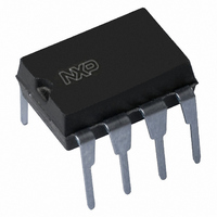
PCF8563P/F4,112 NXP Semiconductors, PCF8563P/F4,112 Datasheet - Page 23

PCF8563P/F4,112
Manufacturer Part Number
PCF8563P/F4,112
Description
IC REAL TIME CLK/CALENDAR 8-DIP
Manufacturer
NXP Semiconductors
Type
Clock/Calendarr
Datasheet
1.PCF8563TF4118.pdf
(45 pages)
Specifications of PCF8563P/F4,112
Package / Case
8-DIP (0.300", 7.62mm)
Time Format
HH:MM:SS (24 hr)
Date Format
YY-MM-DD-dd
Interface
I²C, 2-Wire Serial
Voltage - Supply
1.8 V ~ 5.5 V
Operating Temperature
-40°C ~ 85°C
Mounting Type
Through Hole
Function
Clock/Calendar/Alarm/Timer/Interrupt
Supply Voltage (max)
5.5 V
Supply Voltage (min)
1.8 V
Maximum Operating Temperature
+ 85 C
Minimum Operating Temperature
- 40 C
Mounting Style
Through Hole
Rtc Bus Interface
Serial (2-Wire, I2C)
Lead Free Status / RoHS Status
Lead free / RoHS Compliant
For Use With
568-3615 - DEMO BOARD I2C
Memory Size
-
Lead Free Status / Rohs Status
Lead free / RoHS Compliant
Other names
568-1067-5
935262218112
PCF8563PN
935262218112
PCF8563PN
NXP Semiconductors
PCF8563
Product data sheet
9.5.1 Addressing
9.5.2 Clock and calendar READ or WRITE cycles
9.5 I
Before any data is transmitted on the I
addressed first. The addressing is always carried out with the first byte transmitted after
the start procedure.
The PCF8563 acts as a slave receiver or slave transmitter. Therefore the clock signal SCL
is only an input signal, but the data signal SDA is a bidirectional line.
Two slave addresses are reserved for the PCF8563:
The PCF8563 slave address is illustrated in
The I
Figure
which register is to be accessed next. The upper four bits of the register address are not
used.
2
Fig 18. Slave address
Fig 19. Master transmits to slave receiver (WRITE mode)
C-bus protocol
Read: A3h (10100011)
Write: A2h (10100010)
2
C-bus configuration for the different PCF8563 READ and WRITE cycles is shown in
19,
Figure 20
S
SLAVE ADDRESS
All information provided in this document is subject to legal disclaimers.
and
Rev. 8 — 18 November 2010
Figure
acknowledgement
R/W
from slave
0 A
1
21. The register address is a 4-bit value that defines
REGISTER ADDRESS A
group 1
0
2
1
C-bus, the device which should respond is
0
Figure
0
acknowledgement
group 2
from slave
0
18.
1
mce189
R/W
n bytes
DATA
Real-time clock/calendar
memory register address
auto increment
acknowledgement
from slave
PCF8563
© NXP B.V. 2010. All rights reserved.
A
013aaa346
P
23 of 45


