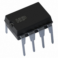
PCF8563P/F4,112 NXP Semiconductors, PCF8563P/F4,112 Datasheet - Page 31

PCF8563P/F4,112
Manufacturer Part Number
PCF8563P/F4,112
Description
IC REAL TIME CLK/CALENDAR 8-DIP
Manufacturer
NXP Semiconductors
Type
Clock/Calendarr
Datasheet
1.PCF8563TF4118.pdf
(45 pages)
Specifications of PCF8563P/F4,112
Package / Case
8-DIP (0.300", 7.62mm)
Time Format
HH:MM:SS (24 hr)
Date Format
YY-MM-DD-dd
Interface
I²C, 2-Wire Serial
Voltage - Supply
1.8 V ~ 5.5 V
Operating Temperature
-40°C ~ 85°C
Mounting Type
Through Hole
Function
Clock/Calendar/Alarm/Timer/Interrupt
Supply Voltage (max)
5.5 V
Supply Voltage (min)
1.8 V
Maximum Operating Temperature
+ 85 C
Minimum Operating Temperature
- 40 C
Mounting Style
Through Hole
Rtc Bus Interface
Serial (2-Wire, I2C)
Lead Free Status / RoHS Status
Lead free / RoHS Compliant
For Use With
568-3615 - DEMO BOARD I2C
Memory Size
-
Lead Free Status / Rohs Status
Lead free / RoHS Compliant
Other names
568-1067-5
935262218112
PCF8563PN
935262218112
PCF8563PN
NXP Semiconductors
13. Dynamic characteristics
Table 30.
V
specified.
[1]
[2]
[3]
[4]
[5]
PCF8563
Product data sheet
Symbol
Oscillator
C
Δf
Quartz crystal parameters (f = 32.768 kHz)
R
C
C
CLKOUT output
δ
I
f
t
t
t
t
t
t
C
t
t
t
t
2
SCL
HD;STA
SU;STA
LOW
HIGH
r
f
SU;DAT
HD;DAT
SU;STO
w(spike)
DD
CLKOUT
C-bus timing characteristics (see
OSCO
s
L
trim
b
osc
= 1.8 V to 5.5 V; V
C
Unspecified for f
All timing values are valid within the operating supply voltage at ambient temperature and referenced to V
swing of V
A detailed description of the I
I
2
/f
C-bus access time between two STARTs or between a START and a STOP condition to this device must be less than one second.
L
osc
is a calculation of C
Dynamic characteristics
SS
Parameter
capacitance on pin OSCO
relative oscillator frequency variation
series resistance
load capacitance
trimmer capacitance
duty cycle on pin CLKOUT
SCL clock frequency
hold time (repeated) START condition
set-up time for a repeated START condition
LOW period of the SCL clock
HIGH period of the SCL clock
rise time of both SDA and SCL signals
fall time of both SDA and SCL signals
capacitive load for each bus line
data set-up time
data hold time
set-up time for STOP condition
spike pulse width
to V
CLKOUT
DD
.
SS
trim
= 32.768 kHz.
= 0 V; T
and C
2
C-bus specification is given in
OSCO
amb
=
Figure
in series:
−
40
All information provided in this document is subject to legal disclaimers.
°
C to +85
28)
C
L
[3][4]
Rev. 8 — 18 November 2010
=
-----------------------------------------
(
(
°
C
C
C; f
trim
trim
Ref. 11
osc
+
⋅
Conditions
ΔV
T
parallel
external;
on pin OSCI
on bus
C
C
= 32.768 kHz; quartz R
amb
OSCO
OSCO
DD
“UM10204”.
= 25 °C
= 200 mV;
)
)
.
[1]
[2]
[5]
s
-
0.6
0.6
1.3
0.6
0
-
Min
15
-
7
5
-
-
-
-
-
100
0.6
= 40 k
Ω
; C
Real-time clock/calendar
-
-
-
-
-
Typ
25
0.2
-
-
50
-
-
-
-
-
-
-
-
IL
L
and V
= 8 pF; unless otherwise
PCF8563
© NXP B.V. 2010. All rights reserved.
IH
with an input voltage
Max
35
-
100
12.5
25
-
400
-
-
-
-
400
-
-
50
0.3
0.3
-
ns
ns
Unit
pF
ppm
kΩ
pF
pF
%
kHz
μs
μs
μs
μs
μs
μs
pF
ns
μs
31 of 45


