ISL1219IUZ Intersil, ISL1219IUZ Datasheet - Page 9
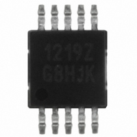
ISL1219IUZ
Manufacturer Part Number
ISL1219IUZ
Description
IC RTC LP BATT BACK SRAM 10MSOP
Manufacturer
Intersil
Type
Clock/Calendar/NVSRAMr
Specifications of ISL1219IUZ
Memory Size
2B
Time Format
HH:MM:SS (12/24 hr)
Date Format
YY-MM-DD-dd
Interface
I²C, 2-Wire Serial
Voltage - Supply
2.7 V ~ 5.5 V
Operating Temperature
-40°C ~ 85°C
Mounting Type
Surface Mount
Package / Case
10-MSOP, Micro10™, 10-uMAX, 10-uSOP
Clock Format
HH
Clock Ic Type
RTC
Interface Type
I2C, Serial
Memory Configuration
2 X 8
Supply Voltage Range
2.7V To 5.5V
Digital Ic Case Style
MSOP
Rohs Compliant
Yes
Lead Free Status / RoHS Status
Lead free / RoHS Compliant
Available stocks
Company
Part Number
Manufacturer
Quantity
Price
Company:

Part Number:
ISL1219IUZ
Manufacturer:
Intersil
Quantity:
490
Company:
Part Number:
ISL1219IUZ
Manufacturer:
Intersil
Quantity:
222
Part Number:
ISL1219IUZ-T
Manufacturer:
INTERSIL
Quantity:
20 000


The I
lower power. Aside from this, all RTC functions are
operational during battery backup mode. Except for SCL and
SDA, all the inputs and outputs of the ISL1219 are active
during battery backup mode unless disabled via the control
register. The User SRAM is operational in battery backup
mode down to 1.8V.
Power Failure Detection
The ISL1219 provides a Real Time Clock Failure Bit (RTCF)
to detect total power failure. It allows users to determine if
the device has powered up after having lost all power to the
device (both V
Low Power Mode
The normal power switching of the ISL1219 is designed to
switch into battery backup mode only if the V
lost. This will ensure that the device can accept a wide range
of backup voltages from many types of sources while reliably
switching into backup mode. Another mode, called Low
Power Mode, is available to allow direct switching from V
to V
the additional monitoring of V
needed, that circuitry is shut down and less power is used
while operating from V
600nA at V
LPMODE bit in the control and status registers.
Low Power Mode is useful in systems where V
higher than V
V
of hysteresis to prevent any switchback of V
switchover. In a system with a V
battery of V
DD
FIGURE 12. BATTERY SWITCHOVER WHEN V
V
BAT
V
V
2
to V
TRIP
DD
BAT
C bus is deactivated in battery backup mode to provide
without requiring V
BAT
DD
BAT
V
when V
BAT
TRIP
DD
= 5V. Low Power Mode is activated via the
= 3V, Low Power Mode can be used.
at all times. The device will switch from
and V
DD
DD
BATTERY BACKUP
BAT
drops below V
. Power savings are typically
DD
).
MODE
DD
9
to drop below V
DD
vs. V
= 5V and backup lithium
TRIP
BAT
V
, with about 50mV
TRIP
is no longer
DD
DD
DD
TRIP
BAT
+ V
after
power is
is normally
TRIPHYS
> V
. Since
3.0V
2.2V
TRIP
DD
ISL1219
However, it is not recommended to use Low Power Mode in
a system with V
there is a finite I-R voltage drop in the V
InterSeal
The ISL1219 has the InterSeal™ Battery Saver which
prevents initial battery current drain before it is first used. For
example, battery-backed RTCs are commonly packaged on
a board with a battery connected. In order to preserve
battery life, the ISL1219 will not draw any power from the
battery source until after the device is first powered up from
the V
battery backup mode whenever V
Event/Tamper Monitor and Detection
The ISL1219 provides an event detection, time stamp and
alarm function to be used in a wide variety of applications
ranging from security, warranty monitoring, data collection
and recording.
The tamper detect input pin, EVIN, can be used as a event
or tamper detection input of an external switch (mechanical
or electronic). When the EVIN pin is a valid HIGH, the
ISL1219 sets the EVT bit in the status register and, can
optionally:
To allow for flexibility of external switches used at the EVIN
pin, the internal pull-up (~1µA in full on mode) can be
disabled/enabled. This will allow more flexibility depending
on the capacitive and resistive loading at the EVIN pin.
A noise filter option is also provided for the event monitor
circuit. The EVIN pin has a time based filter where the EVIN
signal must be stable for a period of time to trigger a valid
detection. The time hysteresis filter can vary from 0, 3.9ms,
15.2ms or 31.25ms.
For low power applications the event monitor can be
sampled at a user selectable rate. The EVIN pin can be
always ON or periodically sampled with a frequency of 1/4, 1
or 2Hz.
1. Issue an Event output signal (EVDET pin) and store time
2. At the time event occurred, stop the RTC registers from
stamp information in on board SRAM (second, minute,
hour, date, month and year)
advancing.
DD
source. Thereafter, the device will switchover to
™
Battery Saver
DD
= 3.3V ±10%, V
DD
BAT
power is lost.
≥ 3.0V, and when
DD
line.
July 15, 2010
FN6314.2
Related parts for ISL1219IUZ
Image
Part Number
Description
Manufacturer
Datasheet
Request
R

Part Number:
Description:
Real Time Clock/Calendar
Manufacturer:
Intersil Corporation
Datasheet:
Part Number:
Description:
Intersil Corporation [CMOS Serial Controller Interface]
Manufacturer:
Intersil Corporation
Datasheet:
Part Number:
Description:
Manufacturer:
Intersil Corporation
Datasheet:
Part Number:
Description:
357-036-542-201 CARDEDGE 36POS DL .156 BLK LOPRO
Manufacturer:
Intersil Corporation
Datasheet:
Part Number:
Description:
1024-Word x 4-Bit LSI Static RAM
Manufacturer:
Intersil Corporation
Datasheet:
Part Number:
Description:
General Purpose NPN Transistor Arrays FN341.4
Manufacturer:
Intersil Corporation
Datasheet:
Part Number:
Description:
CMOS 16-Bit Microprocessor
Manufacturer:
Intersil Corporation
Datasheet:
Part Number:
Description:
Manufacturer:
Intersil Corporation
Datasheet:
Part Number:
Description:
Manufacturer:
Intersil Corporation
Datasheet:
Part Number:
Description:
Manufacturer:
Intersil Corporation
Datasheet:
Part Number:
Description:
Manufacturer:
Intersil Corporation
Datasheet:
Part Number:
Description:
CMOS 6-Bit Latch and Decoder Memory Interfaces
Manufacturer:
Intersil Corporation
Datasheet:
Part Number:
Description:
CA3046General Purpose NPN Transistor Arrays
Manufacturer:
Intersil Corporation
Datasheet:
Part Number:
Description:
Manufacturer:
Intersil Corporation
Datasheet:
Part Number:
Description:
TR909 DLC/FLC SLIC with Low Power Standby
Manufacturer:
Intersil Corporation
Datasheet: