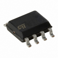
M41T80M6E STMicroelectronics, M41T80M6E Datasheet - Page 12

M41T80M6E
Manufacturer Part Number
M41T80M6E
Description
IC RTC SERIAL W/ALARM 8-SOIC
Manufacturer
STMicroelectronics
Type
Clock/Calendar/Alarmr
Datasheet
1.M41T80M6E.pdf
(25 pages)
Specifications of M41T80M6E
Memory Size
20B
Time Format
HH:MM:SS:hh (24 hr)
Date Format
YY-MM-DD-dd
Interface
I²C, 2-Wire Serial
Voltage - Supply
2 V ~ 5.5 V
Operating Temperature
-40°C ~ 85°C
Mounting Type
Surface Mount
Package / Case
8-SOIC (3.9mm Width)
Function
Clock/Calendar/Alarm/Timer Interrupt
Rtc Memory Size
20 Byte
Supply Voltage (max)
5.5 V
Supply Voltage (min)
2 V
Maximum Operating Temperature
+ 85 C
Minimum Operating Temperature
- 40 C
Mounting Style
SMD/SMT
Rtc Bus Interface
Serial (2-Wire, I2C)
Lead Free Status / RoHS Status
Lead free / RoHS Compliant
Other names
497-2820-5
M41T80M6
M41T80M6
Available stocks
Company
Part Number
Manufacturer
Quantity
Price
Operation
2.3
Figure 10. WRITE mode sequence
12/25
BUS ACTIVITY:
MASTER
SDA LINE
BUS ACTIVITY:
WRITE mode
In this mode the master transmitter transmits to the M41T80 slave receiver. Bus protocol is
shown in
and slave address, a logic '0' (R/W=0) is placed on the bus and indicates to the addressed
device that word address “An” will follow and is to be written to the on-chip address pointer.
The data word to be written to the memory is strobed in next and the internal address
pointer is incremented to the next address location on the reception of an acknowledge
clock. The M41T80 slave receiver will send an acknowledge clock to the master transmitter
after it has received the slave address see
again after it has received the word address and each data byte.
S
Figure 10: WRITE mode sequence on page
ADDRESS
SLAVE
ADDRESS (An)
WORD
Doc ID 9074 Rev 4
DATA n
Figure 7: Slave address location on page 11
12. Following the START condition
DATA n+1
DATA n+X
P
M41T80
AI00591
and


