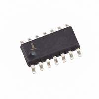
X1228S14 Intersil, X1228S14 Datasheet - Page 21

X1228S14
Manufacturer Part Number
X1228S14
Description
IC RTC CPU SUP WDT 4K EE 14-SOIC
Manufacturer
Intersil
Type
Clock/Calendar/EEPROMr
Datasheet
1.X1228S14-2.7A.pdf
(29 pages)
Specifications of X1228S14
Memory Size
4K (512 x 8)
Time Format
HH:MM:SS (12/24 hr)
Date Format
YY-MM-DD-dd
Interface
I²C, 2-Wire Serial
Voltage - Supply
2.7 V ~ 5.5 V
Operating Temperature
0°C ~ 70°C
Mounting Type
Surface Mount
Package / Case
14-SOIC (3.9mm Width), 14-SOL
Lead Free Status / RoHS Status
Contains lead / RoHS non-compliant
Available stocks
Company
Part Number
Manufacturer
Quantity
Price
Company:
Part Number:
X1228S14
Manufacturer:
Intersil
Quantity:
1
Part Number:
X1228S14I-2.7
Manufacturer:
INTERSIL
Quantity:
20 000
Part Number:
X1228S14I-4.5AT1
Manufacturer:
INTERSIL
Quantity:
20 000
Company:
Part Number:
X1228S14IZ
Manufacturer:
NXP
Quantity:
906
Part Number:
X1228S14IZ-2.7A
Manufacturer:
INTERSIL
Quantity:
20 000
A write to a protected block of memory is ignored, but
will still receive an acknowledge. At the end of the
write command, the X1228 will not initiate an internal
write cycle, and will continue to ACK commands.
Page Write
The X1228 has a page write operation. It is initiated in
the same manner as the byte write operation; but
instead of terminating the write cycle after the first data
byte is transferred, the master can transmit up to 63
more bytes to the memory array and up to 7 more
bytes to the clock/control registers. (Note: Prior to writ-
ing to the CCR, the master must write a 02h, then 06h
to the status register in two preceding operations to
enable the write operation. See “Writing to the
Clock/Control Registers.”
After the receipt of each byte, the X1228 responds with
an acknowledge, and the address is internally incre-
mented by one. When the counter reaches the end of
the page, it “rolls over” and goes back to the first
address on the same page. This means that the master
can write 64 bytes to a memory array page or 8 bytes to
a CCR section starting at any location on that page. For
Figure 13. Page Write Sequence
Signals from
the Master
Signals from
the Slave
SDA Bus
S
a
t
r
t
1
21
Address
Slave
1
1
1
0
C
A
K
0 0 0 0 0 0 0
Address 1
Word
X1228
C
A
K
Address 0
Word
example, if the master begins writing at location 40 of
the memory and loads 30 bytes, then the first 23 bytes
are written to addresses 40 through 63, and the last 7
bytes are written to columns 0 through 6. Afterwards,
the address counter would point to location 7 on the
page that was just written. If the master supplies more
than the maximum bytes in a page, then the previously
loaded data is over written by the new data, one byte at
a time. Refer to Figure 12.
The master terminates the Data Byte loading by issu-
ing a stop condition, which causes the X1228 to begin
the nonvolatile write cycle. As with the byte write oper-
ation, all inputs are disabled until completion of the
internal write cycle. Refer to Figure 13 for the address,
acknowledge, and data transfer sequence.
Stops and Write Modes
Stop conditions that terminate write operations must be
sent by the master after sending at least 1 full data byte
and it’s associated ACK signal. If a stop is issued in the
middle of a data byte, or before 1 full data byte + ACK is
sent, then the X1228 resets itself without performing the
write. The contents of the array are not affected.
C
A
K
1 ≤ n ≤ 64 for EEPROM array
1 ≤ n ≤ 8 for CCR
Data
(1)
Data
(n)
A
C
K
S
o
p
t
May 18, 2006
FN8100.4


