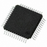
STLC7550TQF7TR STMicroelectronics, STLC7550TQF7TR Datasheet - Page 21

STLC7550TQF7TR
Manufacturer Part Number
STLC7550TQF7TR
Description
IC ANALOG FRONT END LV 48-TQFP
Manufacturer
STMicroelectronics
Datasheet
1.E-STLC7550TQF7.pdf
(24 pages)
Specifications of STLC7550TQF7TR
Number Of Bits
16
Number Of Channels
1
Power (watts)
30mW
Voltage - Supply, Analog
3V
Voltage - Supply, Digital
3V
Package / Case
48-TQFP, 48-VQFP
Lead Free Status / RoHS Status
Lead free / RoHS Compliant
Available stocks
Company
Part Number
Manufacturer
Quantity
Price
Company:
Part Number:
STLC7550TQF7TR
Manufacturer:
STMicroelectronics
Quantity:
10 000
STLC7550
5
Definition and Terminology
Data Transfer Interval
Signal Data
Data Mode
Control Mode
Frame Sync.
Frame Sync and Sampling
Period
ADC Channel
DAC Channel
OverSampling Ratio
Resolution
Dynamic Range
Signal-to-
(Noise+Distortion)
Crosstalk
Power Supply Rejection
Ratio
The time during which data is transfered from D
D
This refers to the input signal and all the converted
representations through the ADC channel and the DAC
channel.
This refers to the data transfer. Since the device is
synchronous, the signal data words from the ADC channel
and to the DAC channel occur simultaneously.
This refers to the digital control data transfer into DIN and
the register read data from D
occurs when requested by hardware or software.
Frame sync refers only to the falling edge of the signal which
initiates the data transfer interval. The primary frame sync
starts the Data Mode and the secondary frame sync starts
the Control Mode.
The time between falling edges of successive primary frame
sync signals.
This term refers to all signal processing circuits between the
analog input and the digital conversion result at D
This term refers to all signal processing circuits between the
digital data word applied to D
analog signal available at OUT+ and OUT-pins.
This term refer to the ratio between the master clock MCLK
corresponding to the oversampling frequency and the
sampling frequency FS.
The number of bits in the input words to the DAC, and the
output words in the ADC.
The S/(N+D) with a 1kHz, -20dBr input signal and
extrapolated to full scale. Use of a small input signal reduces
the harmonic distortion components of the noise to
insignificance. Units in dB or in N
S/(THD+N) is the ratio of the rms of the input signal to the
rms of all other spectral components within the
measurement bandwidth (0.425 x Sampling Frequency).
Units in dB.
The amount of 1kHz signal present on the output of the
grounded input channel with 1kHz 0dB signal present on the
other channel. Units in dB.
PSRR. The amount of 1kHz signal present on the output of
the grounded input channel with 1kHz 200mV
present on the power supply.
IN
. This interval is 16 shift clocks provides by the chip.
Rev 9
OUT
IN
and the differential output
Definition and Terminology
. The control mode interval
bit
as explained before.
PP
OUT
signal
OUT
and to
.
21/24


