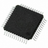
STLC7550TQF7TR STMicroelectronics, STLC7550TQF7TR Datasheet - Page 5

STLC7550TQF7TR
Manufacturer Part Number
STLC7550TQF7TR
Description
IC ANALOG FRONT END LV 48-TQFP
Manufacturer
STMicroelectronics
Datasheet
1.E-STLC7550TQF7.pdf
(24 pages)
Specifications of STLC7550TQF7TR
Number Of Bits
16
Number Of Channels
1
Power (watts)
30mW
Voltage - Supply, Analog
3V
Voltage - Supply, Digital
3V
Package / Case
48-TQFP, 48-VQFP
Lead Free Status / RoHS Status
Lead free / RoHS Compliant
Available stocks
Company
Part Number
Manufacturer
Quantity
Price
Company:
Part Number:
STLC7550TQF7TR
Manufacturer:
STMicroelectronics
Quantity:
10 000
STLC7550
1.1.2
Digital Ground (DGND)
This pin is the ground for DAC and ADC internal digital circuitry.
Host interface (10 pins)
Data In (DIN)
In Data Mode, the data word is the input of the DAC channel. In software, the data word is
followed by the control register word.
Data Out (DOUT)
In Data Mode, the data word is the ADC conversion result. In software, the data word is
followed by the register read.
Frame Synchronization (FS)
In master mode, the frame synchronization signal is used to indicate that the device is ready
to send and receive data. The data transfer begins on the falling edge of the frame-sync
signal. The framesync is generated internally and goes low on the rising edge of SCLK in
master mode. In slave mode the frame is generated externally.
Serial Bit Clock (SCLK)
SCLK clocks the digital data into DIN and out of DOUT during the frame synchronization
interval. The Serial bit clock is generated internally.
Reset Function (RESET)
The reset function is to initialize the internal counters and control register. A minimum low
pulse of 100ns is required to reset the chip. This reset function initiates the serial data
communications. The reset function will initialize all the registers to their default value and
will put the device in a pre-programmed state. After a low-going pulse on RESET, the device
registers will be initialized to provide an over-sampling ratio equal to 160, the serial interface
will be in data mode, the DAC attenuation will be set to infinite, the ADC gain will be set to
0dB, the Differential input mode on the ADC converter will be selected, and the multiplexor
will be set on the main inputs IN+ and IN-. After a reset condition, the first frame
synchronization corresponds to the primary channel.
Power Down (PWRDWN)
The Power-Down input powers down the entire chip (< 50mW). When PWRDWN Pin is
taken low, the device powers down such that the existing internally programmed state is
maintained. When PWRDWN is driven high, full operation resumes after 1ms. If the
PWRDWN input is not used, it should be tied to V
Hardware Control (HC0, HC1)
These two pins are used for Hardware/Software Control of the device. The data on HC0 and
HC1 will be latched on to the device on the rising edge of the Frame Synchronization Pulse.
If these two pins are low, Software Control Mode is selected. When in Software Control
Mode, the LSB of the 16-bit word will select the Data Mode (LSB = 0) or the Control Mode
(LSB = 1). Other combinations of HC0/HC1 are for Hardware Control. These inputs should
be tied low if not used.
Rev 9
DD
.
Pins description & Block diagram
5/24


