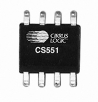
CS5513-BSZ Cirrus Logic Inc, CS5513-BSZ Datasheet - Page 21

CS5513-BSZ
Manufacturer Part Number
CS5513-BSZ
Description
IC ADC 20BIT INTERNAL OSC 8SOIC
Manufacturer
Cirrus Logic Inc
Datasheet
1.CS5513-BSZ.pdf
(26 pages)
Specifications of CS5513-BSZ
Data Interface
Serial
Number Of Bits
20
Sampling Rate (per Second)
326
Number Of Converters
1
Power Dissipation (max)
2.7mW
Voltage Supply Source
Dual ±
Operating Temperature
-40°C ~ 85°C
Mounting Type
Surface Mount
Package / Case
8-SOIC (0.200", 5.30mm Width)
Resolution (bits)
20bit
Sampling Rate
100SPS
Input Channel Type
Differential
Supply Voltage Range - Analog
4.75V To 5.25V
Supply Current
385µA
Digital Ic Case Style
SOIC
Lead Free Status / RoHS Status
Lead free / RoHS Compliant
Other names
598-1707
Available stocks
Company
Part Number
Manufacturer
Quantity
Price
Part Number:
CS5513-BSZ
Manufacturer:
CIRRUS
Quantity:
20 000
3. PIN DESCRIPTIONS
Control Pins and Serial Data I/O
CS - Chip Select, Pin 4
SDO - Serial Data Output, Pin 8
SCLK - Serial Clock Input, Pin 5
Measurement and Reference Inputs
AIN+, AIN- - Differential Analog Input, Pins 2, 3
VREF - Voltage Reference Input, Pin 1
Power Supply Connections
V+ - Positive Power, Pin 6
V- - Negative Supply, Pin 7
DS337F4
CS is a dual function pin, which determines the state of SDO, as well as the digital logic-low output
level. When CS is low, SDO will be active. When high, the SDO pin will output a high-impedance state.
The logic-low level of SDO will match the active-low voltage on CS.
SDO is the serial data output. It will output a high-impedance state if CS = 1. The logic-low level of SDO
will match the active-low voltage on CS.
SCLK is the serial bit-clock which controls the shifting of data from the ADCs. This input goes through a
Schmitt trigger to allow for slow rise and fall time signals. If held high, the device will enter sleep mode.
In the CS5510/12, this input is also used as a master clock source which determines conversion speeds
and throughput. In the CS5511/13, SCLK is only used to read the conversion data and put the part in
sleep mode.
Differential input pins into the device
Input Voltage which establishes the voltage reference, with respect to V-, for the on-chip modulator
Positive supply voltage
Negative supply voltage
VREF
AIN+
AIN-
CS
1
2
3
4
8
7
6
5
SDO
V-
V+
SCLK
CS5510/11/12/13
21


