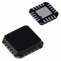
AD7699BCPZ Analog Devices Inc, AD7699BCPZ Datasheet - Page 12

AD7699BCPZ
Manufacturer Part Number
AD7699BCPZ
Description
IC ADC 8CH 16BIT 500KSPS 20LFCSP
Manufacturer
Analog Devices Inc
Datasheet
1.AD7699BCPZ.pdf
(28 pages)
Specifications of AD7699BCPZ
Data Interface
DSP, MICROWIRE™, QSPI™, Serial, SPI™
Number Of Bits
16
Sampling Rate (per Second)
500k
Number Of Converters
1
Power Dissipation (max)
32mW
Voltage Supply Source
Single Supply
Operating Temperature
-40°C ~ 85°C
Mounting Type
Surface Mount
Package / Case
20-VFQFN, CSP Exposed Pad
Resolution (bits)
16bit
Sampling Rate
500kSPS
Input Channel Type
Pseudo Differential, Single Ended
Supply Voltage Range - Analog
4.5V To 5.5V
Lead Free Status / RoHS Status
Lead free / RoHS Compliant
Available stocks
Company
Part Number
Manufacturer
Quantity
Price
Company:
Part Number:
AD7699BCPZ
Manufacturer:
ADI
Quantity:
490
Part Number:
AD7699BCPZ
Manufacturer:
ADI/亚德诺
Quantity:
20 000
AD7699
TERMINOLOGY
Least Significant Bit (LSB)
The LSB is the smallest increment that can be represented by a
converter. For an analog-to-digital converter with N bits of
resolution, the LSB expressed in volts is
Integral Nonlinearity Error (INL)
INL refers to the deviation of each individual code from a line
drawn from negative full scale through positive full scale. The
point used as negative full scale occurs ½ LSB before the first
code transition. Positive full scale is defined as a level 1½ LSB
beyond the last code transition. The deviation is measured from
the middle of each code to the true straight line (see Figure 26).
Differential Nonlinearity Error (DNL)
In an ideal ADC, code transitions are 1 LSB apart. DNL is the
maximum deviation from this ideal value. It is often specified in
terms of resolution for which no missing codes are guaranteed.
Offset Error
For unipolar mode, the first transition should occur at a level
½ LSB above analog ground. The unipolar offset error is the
deviation of the actual transition from that point. For bipolar
mode, the first transition should occur at a level ½ LSB above
V
transition from that point.
Gain Error
The last transition (from 111 … 10 to 111 … 11) should occur
for an analog voltage 1½ LSB below the nominal full scale. The
gain error is the deviation in LSB (or percentage of full-scale
range) of the actual level of the last transition from the ideal
level after the offset error is adjusted out. Closely related is the
full-scale error (also in LSB or percentage of full-scale range),
which includes the effects of the offset error.
Aperture Delay
Aperture delay is the measure of the acquisition performance. It
is the time between the rising edge of the CNV input and the
point at which the input signal is held for a conversion.
Transient Response
Transient response is the time required for the ADC to accurately
acquire its input after a full-scale step function is applied.
Dynamic Range
Dynamic range is the ratio of the rms value of the full scale to
the total rms noise measured with the inputs shorted together.
The value for dynamic range is expressed in decibels.
REF
/2. The bipolar offset error is the deviation of the actual
LSB
(V) =
V
2
REF
N
Rev. 0 | Page 12 of 28
Signal-to-Noise Ratio (SNR)
SNR is the ratio of the rms value of the actual input signal to the
rms sum of all other spectral components below the Nyquist
frequency, excluding harmonics and dc. The value for SNR is
expressed in decibels.
Signal-to-(Noise + Distortion) Ratio (SINAD)
SINAD is the ratio of the rms value of the actual input signal to
the rms sum of all other spectral components below the Nyquist
frequency, including harmonics but excluding dc. The value for
SINAD is expressed in decibels.
Total Harmonic Distortion (THD)
THD is the ratio of the rms sum of the first five harmonic
components to the rms value of a full-scale input signal and is
expressed in decibels.
Spurious-Free Dynamic Range (SFDR)
SFDR is the difference, in decibels, between the rms amplitude
of the input signal and the peak spurious signal.
Effective Number of Bits (ENOB)
ENOB is a measurement of the resolution with a sine wave
input. It is related to SINAD by the formula
and is expressed in bits.
Channel-to-Channel Crosstalk
Channel-to-channel crosstalk is a measure of the level of crosstalk
between any two adjacent channels. It is measured by applying a
dc to the channel under test and applying a full-scale, 100 kHz
sine wave signal to the adjacent channel(s). The crosstalk is the
amount of signal that leaks into the test channel and is expressed
in decibels.
Reference Voltage Temperature Coefficient
Reference voltage temperature coefficient is derived from the
typical shift of output voltage at 25°C on a sample of parts at the
maximum and minimum reference output voltage (V
ured at T
where:
V
V
V
T
T
MAX
MIN
REF
REF
REF
ENOB = (SINAD
(Max) = maximum V
(Min) = minimum V
(25°C) = V
= –40°C.
TCV
= +85°C.
MIN
REF
, T (25°C), and T
(
ppm/
REF
°
at 25°C.
) C
dB
=
− 1.76)/6.02
V
REF
REF
V
REF
MAX
REF
at T
(
at T
25
. It is expressed in ppm/°C as
(
Max
°
MIN
) C
MIN
, T (25°C), or T
×
– )
, T (25°C), or T
(
T
V
MAX
REF
(
–
Min
T
MIN
)
)
×
MAX
MAX
10
REF
.
6
.
) meas-


