AD7699BCPZ Analog Devices Inc, AD7699BCPZ Datasheet - Page 22
AD7699BCPZ
Manufacturer Part Number
AD7699BCPZ
Description
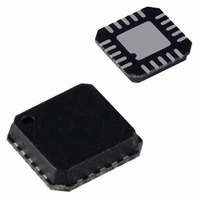
IC ADC 8CH 16BIT 500KSPS 20LFCSP
Manufacturer
Analog Devices Inc
Datasheet
1.AD7699BCPZ.pdf
(28 pages)
Specifications of AD7699BCPZ
Data Interface
DSP, MICROWIRE™, QSPI™, Serial, SPI™
Number Of Bits
16
Sampling Rate (per Second)
500k
Number Of Converters
1
Power Dissipation (max)
32mW
Voltage Supply Source
Single Supply
Operating Temperature
-40°C ~ 85°C
Mounting Type
Surface Mount
Package / Case
20-VFQFN, CSP Exposed Pad
Resolution (bits)
16bit
Sampling Rate
500kSPS
Input Channel Type
Pseudo Differential, Single Ended
Supply Voltage Range - Analog
4.5V To 5.5V
Lead Free Status / RoHS Status
Lead free / RoHS Compliant
Available stocks
Company
Part Number
Manufacturer
Quantity
Price
Company:

Part Number:
AD7699BCPZ
Manufacturer:
ADI
Quantity:
490
Part Number:
AD7699BCPZ
Manufacturer:
ADI/亚德诺
Quantity:
20 000


AD7699
GENERAL TIMING WITHOUT A BUSY INDICATOR
Figure 35 details the timing for all three modes: reading/writing
during conversion, after conversion, and spanning conversion.
Note that the gating item for both CFG and data readback is at
the end of conversion (EOC). At the end of conversions (EOC),
if CNV is high, the busy indicator is disabled.
As detailed previously, the data access should occur up to safe
data reading/writing time, t
written to prior to EOC, it is discarded and the current
configuration remains. If the conversion result is not read out
fully prior to EOC, it is lost as the ADC updates SDO with the
PHASE
SDO
SDO
SDO
CNV
SCK
CNV
SCK
CNV
SCK
NOTES
1. CNV MUST BE HIGH PRIOR TO THE END OF CONVERSION (EOC) TO AVOID THE BUSY INDICATOR.
DIN
DIN
DIN
A TOTAL OF 16 SCK FALLING EDGES IS REQUIRED TO RETURN SDO TO HIGH-Z. IF CFG READBACK
IS ENABLED, A TOTAL OF 30 SCK FALLING EDGES IS REQUIRED TO RETURN SDO TO HIGH-Z.
POWER
UP
CONVERSION (n – 2)
1
t
DATA
t
XXX
XXX
CONV
16/30
DATA
t
CYC
. If the full CFG word was not
ACQUISITION
1
1
Figure 35. General Interface Timing for the AD7699 Without a Busy Indicator
START OF CONVERSION
(n – 1)
CFG (n)
(n – 2)
DATA
DATA
(n – 2)
16/30
(n – 2)
MSB
CFG (n)
CONVERSION (n – 1)
1
DATA (n – 2)
(n – 2)
DATA
16/30
CFG (n)
END OF CONVERSION (EOC)
16/30
Rev. 0 | Page 22 of 28
ACQUISITION
1
1
CFG (n + 1)
(n – 1)
(n)
DATA
DATA
(n – 1)
16/30
(n – 1)
MSB
MSB of the current conversion. For detailed timing, refer to
Figure 36 and Figure 37, which depict reading/writing spanning
conversion with all timing details, including setup, hold, and SCK.
When CNV is brought low after EOC, SDO is driven from high
impedance to the MSB. Falling SCK edges clock out bits starting
with MSB − 1.
The SCK can idle high or low depending on the clock polarity
(CPOL) and clock phase (CPHA) settings if SPI is used. A simple
solution is to use CPOL = CPHA = 0 as shown in Figure 35 with
SCK idling low.
CFG (n + 1)
CONVERSION (n)
1
DATA (n – 1)
CFG (n + 1)
(n – 1)
DATA
16/30
16/30
EOC
ACQUISITION
1
1
CFG (n + 2)
(n + 1)
DATA (n)
DATA (n)
16/30
MSB
(n)
CFG (n + 2)
CONVERSION (n + 1)
1
DATA (n)
CFG (n + 2)
DATA (n)
16/30
16/30
EOC
ACQUISITION
1
1
DATA (n + 1)
CFG (n + 3)
CFG (n + 3)
(n + 2)
(n + 1)
DATA
(n + 1)
MSB
Related parts for AD7699BCPZ
Image
Part Number
Description
Manufacturer
Datasheet
Request
R

Part Number:
Description:
±1.7g Dual-Axis IMEMS Accelerometer Evaluation Board
Manufacturer:
Analog Devices Inc
Datasheet:

Part Number:
Description:
Inertial Sensor Evaluation System
Manufacturer:
Analog Devices Inc
Datasheet:
Part Number:
Description:
Manufacturer:
Analog Devices Inc
Datasheet:
Part Number:
Description:
Manufacturer:
Analog Devices Inc
Datasheet:
Part Number:
Description:
Manufacturer:
Analog Devices Inc
Datasheet:
Part Number:
Description:
Manufacturer:
Analog Devices Inc
Datasheet:
Part Number:
Description:
Manufacturer:
Analog Devices Inc
Datasheet:
Part Number:
Description:
Manufacturer:
Analog Devices Inc
Datasheet:
Part Number:
Description:
Manufacturer:
Analog Devices Inc
Datasheet:
Part Number:
Description:
Manufacturer:
Analog Devices Inc
Datasheet:
Part Number:
Description:
Manufacturer:
Analog Devices Inc
Datasheet:
Part Number:
Description:
Manufacturer:
Analog Devices Inc
Datasheet:
Part Number:
Description:
Manufacturer:
Analog Devices Inc
Datasheet: