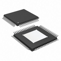
AD7760BSVZ Analog Devices Inc, AD7760BSVZ Datasheet - Page 23

AD7760BSVZ
Manufacturer Part Number
AD7760BSVZ
Description
IC ADC 24BIT 2.5MSPS 64TQFP
Manufacturer
Analog Devices Inc
Datasheet
1.AD7760BSVZ.pdf
(36 pages)
Specifications of AD7760BSVZ
Data Interface
Parallel
Number Of Bits
24
Sampling Rate (per Second)
2.5M
Number Of Converters
1
Power Dissipation (max)
958mW
Voltage Supply Source
Analog and Digital
Operating Temperature
-40°C ~ 85°C
Mounting Type
Surface Mount
Package / Case
64-TQFP Exposed Pad
Resolution (bits)
24bit
Sampling Rate
2.5MSPS
Input Channel Type
Differential
Supply Voltage Range - Digital
2.375V To 2.625V
Supply Current
49mA
Lead Free Status / RoHS Status
Lead free / RoHS Compliant
Available stocks
Company
Part Number
Manufacturer
Quantity
Price
Company:
Part Number:
AD7760BSVZ
Manufacturer:
Analog Devices Inc
Quantity:
10 000
Part Number:
AD7760BSVZ
Manufacturer:
ADI/亚德诺
Quantity:
20 000
Company:
Part Number:
AD7760BSVZ-REEL
Manufacturer:
Analog Devices Inc
Quantity:
10 000
WRITING TO THE AD7760
There are many features and parameters that the user can
change by writing to the AD7760 device. See the Using the
AD7760 section, which details the writing sequence needed to
initialize the operation of the part.
The AD7760 has programmable registers that are 16 bits wide.
This means that two write operations are required to program a
register. The first write contains the register address, and the
second write contains the register data. An exception is when a
user-defined filter is being downloaded to the AD7760. This is
described in detail in the Downloading a User-Defined Filter
section. The AD7760 Registers section contains the register
addresses and details.
Rev. A | Page 23 of 36
Figure 3 shows a write operation to the AD7760. The RD /WR
line is held high while the CS line is brought low for a minimum
of four ICLK periods. The register address is latched during this
period. The CS line is brought high again for a minimum of
four ICLK periods before the register data is put onto the data
bus. If a read operation occurs between the writing of the
register address and the register data, the register address is
cleared and the next write must be the register address. This
also provides a method to revert back to a known situation if
the user forgets whether the next write is an address or data.
Generally, the AD7760 is written to and configured on power-
up and very infrequently, if at all, after that. Following any write
operation, the full group delay of the filter must elapse before
valid data is output from the AD7760.
AD7760


