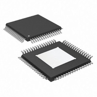
AD7760BSVZ Analog Devices Inc, AD7760BSVZ Datasheet - Page 34

AD7760BSVZ
Manufacturer Part Number
AD7760BSVZ
Description
IC ADC 24BIT 2.5MSPS 64TQFP
Manufacturer
Analog Devices Inc
Datasheet
1.AD7760BSVZ.pdf
(36 pages)
Specifications of AD7760BSVZ
Data Interface
Parallel
Number Of Bits
24
Sampling Rate (per Second)
2.5M
Number Of Converters
1
Power Dissipation (max)
958mW
Voltage Supply Source
Analog and Digital
Operating Temperature
-40°C ~ 85°C
Mounting Type
Surface Mount
Package / Case
64-TQFP Exposed Pad
Resolution (bits)
24bit
Sampling Rate
2.5MSPS
Input Channel Type
Differential
Supply Voltage Range - Digital
2.375V To 2.625V
Supply Current
49mA
Lead Free Status / RoHS Status
Lead free / RoHS Compliant
Available stocks
Company
Part Number
Manufacturer
Quantity
Price
Company:
Part Number:
AD7760BSVZ
Manufacturer:
Analog Devices Inc
Quantity:
10 000
Part Number:
AD7760BSVZ
Manufacturer:
ADI/亚德诺
Quantity:
20 000
Company:
Part Number:
AD7760BSVZ-REEL
Manufacturer:
Analog Devices Inc
Quantity:
10 000
AD7760
STATUS REGISTER (READ ONLY)
MSB
D15
PART 1
Table 17. Bit Descriptions of Status Register
Bit
15, 14
13 to 11
10
9
8
7
6
5
4
3
2 to 0
OFFSET REGISTER—ADDRESS 0x0003
Non-bit-mapped, Default Value 0x0000
The offset register uses twos complement notation and is scaled
such that 0x7FFF (maximum positive value) and 0x8000 (max-
imum negative value) correspond to an offset of +0.78125% and
−0.78125%, respectively. Offset correction is applied after any
gain correction. Using the default gain value of 1.25 and assuming
a reference voltage of 4.096 V, the offset correction range is
approximately ±25 mV.
GAIN REGISTER—ADDRESS 0x0004
Non-bit-mapped, Default Value 0xA000
The gain register is scaled such that 0x8000 corresponds to a
gain of 1.0. The default value of this register is 1.25 (0xA000).
This results in a full-scale digital output when the input is at
80% of V
±80% of V
REF
D14
PART 0
REF
Mnemonic
PART [1:0]
DIE [2:0]
0
LPWR
OVR
DL_OK
FILTOK
UFILT
BYP F3
BYP F1
DEC [2:0]
, tying in with the maximum analog input range of
p-p.
D13
DIE 2
D12
DIE 1
Comment
Part Number. These bits are constant for the AD7760.
Die Number. These bits reflect the current AD7760 die number for identification purposes within a system.
This bit is set to 0.
Low Power. If the AD7760 is operating in low power mode, this bit is set to 1.
If the current analog input exceeds the current overrange threshold, this bit is set.
When downloading a user filter to the AD7760, a checksum is generated. This checksum is compared to the one
downloaded following the coefficients. If these checksums agree, this bit is set.
When a user-defined filter is in use, a checksum is generated when the filter coefficients pass through the filter. This
generated checksum is compared to the one downloaded. If they match, this bit is set.
If a user-defined filter is in use, this bit is set.
Bypass Filter 3. If Filter 3 is bypassed by setting the relevant bit in Control Register 1, this bit is also set.
Bypass Filter 1. If Filter 1 is bypassed by setting the relevant bit in Control Register 1, this bit is also set.
Decimation Rate. These bits correspond to the bits set in Control Register 1.
D11
DIE 0
D10
0
D9
LPWR
D8
OVR
Rev. A | Page 34 of 36
D7
DL_OK
OVERRANGE REGISTER—ADDRESS 0x0005
Non-bit-mapped, Default Value 0xCCCC
The overrange register value is compared with the output of
the first decimation filter to obtain an overload indication with
minimum propagation delay. This is prior to any gain scaling
or offset adjustment. The default value is 0xCCCC, which
corresponds to 80% of V
input voltage). Assuming V
the input voltage exceeds approximately 6.55 V p-p differential.
Once the overrange bit is set, the DVALID bit in the status bits
of the AD7760 ouptut is set to zero, providing another indication
that an input overrange has occurred. Note that the overrange
bit is set immediately if the analog input voltage exceeds 100% of
V
REF
D6
FILTOK
for more than four consecutive samples at the modulator rate.
D5
UFILT
D4
BYP F3
REF
REF
(the maximum permitted analog
= 4.096 V, the bit is then set when
D3
BYP F1
D2
DEC2
D1
DEC1
LSB
D0
DEC0


