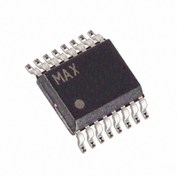
MAX11604EEE+ Maxim Integrated Products, MAX11604EEE+ Datasheet - Page 13

MAX11604EEE+
Manufacturer Part Number
MAX11604EEE+
Description
IC ADC SERIAL 8BIT 12CH 16-QSOP
Manufacturer
Maxim Integrated Products
Datasheet
1.MAX11602EEE.pdf
(23 pages)
Specifications of MAX11604EEE+
Number Of Bits
8
Sampling Rate (per Second)
188k
Data Interface
I²C, Serial
Number Of Converters
1
Power Dissipation (max)
1.75mW
Voltage Supply Source
Single Supply
Operating Temperature
-40°C ~ 85°C
Mounting Type
Surface Mount
Package / Case
16-SSOP (0.150", 3.90mm Width)
Resolution
8 bit
Interface Type
I2C
Snr
49 dB
Voltage Reference
4.096 V
Supply Voltage (max)
5.5 V
Supply Voltage (min)
4.5 V
Maximum Power Dissipation
666.7 mW
Maximum Operating Temperature
+ 85 C
Mounting Style
SMD/SMT
Input Voltage
5 V
Minimum Operating Temperature
- 40 C
Lead Free Status / RoHS Status
Lead free / RoHS Compliant
A read cycle must be initiated to obtain conversion
results. Read cycles begin with the bus master issuing
a START condition followed by 7 address bits and a
read bit (R/W = 1). If the address byte is successfully
received, the MAX11600–MAX11605 (slave) issue an
acknowledge. The master then reads from the slave.
After the master has received the results, it can issue
an acknowledge if it wants to continue reading or a not
acknowledge if it no longer wishes to read. If the
MAX11600–MAX11605 receive a not acknowledge,
they release SDA, allowing the master to generate a
STOP or repeated START. See the Clock Mode and
Scan Mode sections for detailed information on how
data is obtained and converted.
Figure 7. Slave Address Byte
Figure 8. F/S Mode to HS Mode Transfer
SDA
SCL
S
2.7V to 3.6V and 4.5V to 5.5V, Low-Power,
SDA
SCL
4-/8-/12-Channel 2-Wire Serial 8-Bit ADCs
______________________________________________________________________________________
MAX11600/MAX11601
MAX11602/MAX11603
MAX11604/MAX11605
0
S
DEVICE
1
0
1
Data Byte (Read Cycle)
1
0
2
SLAVE ADDRESS
1100100
1101101
1100101
HS MODE MASTER CODE
0
0
3
SLAVE ADDRESS
F/S MODE
0
1
4
1
X
5
The clock mode determines the conversion clock, the
acquisition time, and the conversion time. The clock
mode also affects the scan mode. The state of the
setup byte’s CLK bit determines the clock mode (Table
1). At power-up, the MAX11600–MAX11605 default to
internal clock mode (CLK = zero).
When configured for internal clock mode (CLK = zero),
the MAX11600–MAX11605 use their internal oscillator
as the conversion clock. In internal clock mode, the
MAX11600–MAX11605 begin tracking analog input on
the ninth falling clock edge of a valid slave address
byte. Two internal clock cycles later, the analog signal
is acquired and the conversion begins. While tracking
and converting the analog input signal, the
MAX11600–MAX11605 hold SCL low (clock stretching).
After the conversion completes, the results are stored in
0
X
6
0
X
7
R/W
A
8
A
9
Sr
HS MODE
Internal Clock
Clock Mode
13


