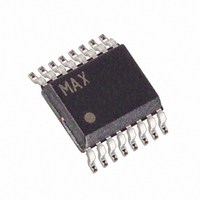
MAX11604EEE+ Maxim Integrated Products, MAX11604EEE+ Datasheet - Page 5

MAX11604EEE+
Manufacturer Part Number
MAX11604EEE+
Description
IC ADC SERIAL 8BIT 12CH 16-QSOP
Manufacturer
Maxim Integrated Products
Datasheet
1.MAX11602EEE.pdf
(23 pages)
Specifications of MAX11604EEE+
Number Of Bits
8
Sampling Rate (per Second)
188k
Data Interface
I²C, Serial
Number Of Converters
1
Power Dissipation (max)
1.75mW
Voltage Supply Source
Single Supply
Operating Temperature
-40°C ~ 85°C
Mounting Type
Surface Mount
Package / Case
16-SSOP (0.150", 3.90mm Width)
Resolution
8 bit
Interface Type
I2C
Snr
49 dB
Voltage Reference
4.096 V
Supply Voltage (max)
5.5 V
Supply Voltage (min)
4.5 V
Maximum Power Dissipation
666.7 mW
Maximum Operating Temperature
+ 85 C
Mounting Style
SMD/SMT
Input Voltage
5 V
Minimum Operating Temperature
- 40 C
Lead Free Status / RoHS Status
Lead free / RoHS Compliant
ELECTRICAL CHARACTERISTICS (continued)
(V
V
1.7MHz, T
Note 1: The MAX11600/MAX11602/MAX11604 are tested at V
Note 2: Relative accuracy is the deviation of the analog value at any code from its theoretical value after the full-scale range and
Note 3: Offset nulled.
Note 4: Ground on channel; sine wave applied to all off channels.
Note 5: Conversion time is defined as the number of clock cycles (eight) multiplied by the clock period. Conversion time does not
Note 6: The absolute voltage range for the analog inputs (AIN0–AIN11) is from GND to V
Note 7: When AIN_/REF (MAX11600/MAX11601/MAX11604/MAX11605) or REF (MAX11602/MAX11603) is configured to be an inter-
Note 8: The switch connecting the reference buffer to AIN_/REF or REF has a typical on-resistance of 675Ω.
Note 9: ADC performance is limited by the converter’s noise floor, typically 1.4mV
Note 10: Electrical characteristics are guaranteed from V
Note 11: Power-supply rejection ratio is measured as:
Note 12: A master device must provide a data hold time for SDA (referred to V
Note 13: C
Note 14: f
Data Hold Time
Data Setup Time
Rise Time of SCL Signal
(Current Source Enabled)
Rise Time of SCL Signal After
Acknowledge Bit
Fall Time of SCL Signal
Rise Time of SDA Signal
Fall Time of SDA Signal
Setup Time for STOP Condition
Capacitive Load for Each Bus Line
Pulse Width of Spike Suppressed
REF
DD
= 2.7V to 3.6V (MAX11601/MAX11603/MAX11605), V
= 2.048V (MAX11601/MAX11603/MAX11605), V
= 3V. All devices are configured for unipolar, single-ended inputs.
offsets have been calibrated.
include acquisition time. SCL is the conversion clock in the external clock mode.
nal reference (SEL[2:1] = 11), decouple AIN_/REF or REF to GND with a 0.01µF capacitor.
Operating Characteristics .
for the MAX11601/MAX11603/MAX11605, where N is the number of bits.
specified at T
Power-supply rejection ratio is measured as:
for the MAX11600/MAX11602/MAX11604, where N is the number of bits.
SCL’s falling edge (Figure 1).
A
PARAMETER
[
SCLH
[
V
V
B
= T
FS
FS
= total capacitance of one bus line in pF. t
(
(
MIN
5 5
3 3
must meet the minimum clock low time plus the rise/fall times.
2.7V to 3.6V and 4.5V to 5.5V, Low-Power,
.
.
V
V
to T
)
5 5
4-/8-/12-Channel 2-Wire Serial 8-Bit ADCs
)
3 3
_______________________________________________________________________________________
−
.
−
.
V
A
V
V
MAX
V
FS
FS
−
= +25°C with C
−
(
4 5
(
2 7
4 5
, unless otherwise noted. Typical values are at T
2 7
.
.
.
.
V
V
V
V
)
)
]
]
×
×
V
V
2
REF
2
REF
SYMBOL
N
t
N
t
t
SU
HD
SU
t
t
t
RCL1
t
t
RDA
RCL
FCL
FDA
C
t
B
,
SP
.
.
DAT
DAT
B
,
,
STO
= 400pF.
(Note 12)
(Note 13)
(Note 13)
(Note 13)
(Note 13)
(Note 13)
R
REF
, t
DD(MIN)
FDA
DD
= 4.096V (MAX11600/MAX11602/MAX11604). External clock, f
= 4.5V to 5.5V (MAX11600/MAX11602/MAX11604). External reference,
, and t
DD
CONDITIONS
to V
= 5V and the MAX11601/MAX11603/MAX11605 are tested at V
F
DD(MAX)
measured between 0.3V
A
= +25°C.)
. For operation beyond this range, see the Typical
IL
of SCL) to bridge the undefined region of
P-P
.
DD
.
DD
MIN
and 0.7V
160
10
20
20
20
20
20
0
0
DD
TYP
. The minimum value is
MAX
150
160
160
160
400
80
80
10
UNITS
SCL
pF
ns
ns
ns
ns
ns
ns
ns
ns
ns
DD
5
=


