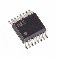
MAX11604EEE+ Maxim Integrated Products, MAX11604EEE+ Datasheet - Page 9

MAX11604EEE+
Manufacturer Part Number
MAX11604EEE+
Description
IC ADC SERIAL 8BIT 12CH 16-QSOP
Manufacturer
Maxim Integrated Products
Datasheet
1.MAX11602EEE.pdf
(23 pages)
Specifications of MAX11604EEE+
Number Of Bits
8
Sampling Rate (per Second)
188k
Data Interface
I²C, Serial
Number Of Converters
1
Power Dissipation (max)
1.75mW
Voltage Supply Source
Single Supply
Operating Temperature
-40°C ~ 85°C
Mounting Type
Surface Mount
Package / Case
16-SSOP (0.150", 3.90mm Width)
Resolution
8 bit
Interface Type
I2C
Snr
49 dB
Voltage Reference
4.096 V
Supply Voltage (max)
5.5 V
Supply Voltage (min)
4.5 V
Maximum Power Dissipation
666.7 mW
Maximum Operating Temperature
+ 85 C
Mounting Style
SMD/SMT
Input Voltage
5 V
Minimum Operating Temperature
- 40 C
Lead Free Status / RoHS Status
Lead free / RoHS Compliant
minimize sampling errors with higher source imped-
ances, connect a 100pF capacitor from the analog
input to GND. This input capacitor forms an RC filter
with the source impedance limiting the analog input
bandwidth. For larger source impedances, use a buffer
amplifier to maintain analog input signal integrity.
When operating in internal clock mode, the T/H circuitry
enters its tracking mode on the ninth falling clock edge
of the address byte (see the Slave Address section).
The T/H circuitry enters hold mode two internal clock
cycles later. A conversion or a series of conversions is
then internally clocked (eight clock cycles per conver-
sion) and the MAX11600–MAX11605 hold SCL low.
When operating in external clock mode, the T/H circuit-
ry enters track mode on the seventh falling edge of a
valid slave address byte. Hold mode is then entered on
the falling edge of the eighth clock cycle. The conver-
sion is performed during the next eight clock cycles.
The time required for the T/H circuitry to acquire an
input signal is a function of input capacitance. If the
analog input source impedance is high, the acquisition
time lengthens and more time must be allowed
between conversions. The acquisition time (t
minimum time needed for the signal to be acquired. It is
calculated by:
Figure 1. I
a) F/S-MODE I
b) HS-MODE I
SDA
SDA
SCL
SCL
2
C Serial-Interface Timing
S
S
t
t
HD.STA
HD.STA
2
2
C SERIAL-INTERFACE TIMING
C SERIAL-INTERFACE TIMING
2.7V to 3.6V and 4.5V to 5.5V, Low-Power,
4-/8-/12-Channel 2-Wire Serial 8-Bit ADCs
_______________________________________________________________________________________
t
t
LOW
LOW
t
RCL
t
R
t
SU.DAT
t
SU.DAT
t
t
HIGH
HIGH
t
FCL
t
F
t
HD.DAT
t
HD.DAT
ACQ
) is the
HS MODE
t
t
SU.STA
SU.STA
where R
R
clock mode. For internal clock mode, the acquisition
time is two internal clock cycles. To select R
allow 625ns for t
for clock frequency variations.
Figure 2. Load Circuit
IN
Sr
Sr
= 2.5kΩ, and C
t
HD.STA
t
HD.STA
SOURCE
t
ACQ
SDA
≥ 6.25
A
A
ACQ
is the analog input source impedance,
IN
in internal clock mode to account
= 18pF. t
(R
V
DD
SOURCE
t
RCL1
t
t
SU.STO
SU.STO
I
I
OH
OL
t
RDA
= 3mA
= 0mA
ACQ
+ R
400pF
is 1/f
t
V
R
OUT
P
IN
t
t
BUF
BUF
)
SCL
F/S MODE
C
t
F
IN
for external
S
S
t
SOURCE
t
FDA
9
,


