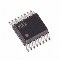
MAX1167BEEE+ Maxim Integrated Products, MAX1167BEEE+ Datasheet - Page 24

MAX1167BEEE+
Manufacturer Part Number
MAX1167BEEE+
Description
IC ADC 16BIT 200KSPS 16-QSOP
Manufacturer
Maxim Integrated Products
Datasheet
1.MAX1167BEEE.pdf
(30 pages)
Specifications of MAX1167BEEE+
Number Of Bits
16
Sampling Rate (per Second)
200k
Data Interface
MICROWIRE™, QSPI™, Serial, SPI™
Number Of Converters
1
Power Dissipation (max)
667mW
Voltage Supply Source
Analog and Digital
Operating Temperature
-40°C ~ 85°C
Mounting Type
Surface Mount
Package / Case
16-SSOP (0.150", 3.90mm Width)
Lead Free Status / RoHS Status
Lead free / RoHS Compliant
The internal bandgap reference provides a buffered
+4.096V. Bypass REFCAP with a 0.1µF capacitor to
AGND and REF with a 1µF capacitor to AGND. For best
results, use low-ESR, X5R/X7R ceramic capacitors.
Allow 5ms for the reference and buffer to wake up from
full power-down (see Table 5).
The MAX1167/MAX1168 accept an external reference
with a voltage range between +3.8V and AV
the external reference directly to REF. Bypass REF to
AGND with a 10µF capacitor. When not using a low-ESR
bypass capacitor, use a 0.1µF ceramic capacitor in paral-
lel with the 10µF capacitor. Noise on the reference
degrades conversion accuracy.
The input impedance at REF is 37kΩ for DC currents.
During a conversion, the external reference at REF
must deliver 118µA of DC load current and have an out-
put impedance of 10Ω or less.
For optimal performance, buffer the reference through
an op amp and bypass the REF input. Consider the
equivalent input noise (40µV
MAX1168 when choosing a reference.
Select either an external (0.1MHz to 4.8MHz) or the
internal 4MHz (typ) clock to perform conversions
(Table 6). The external clock shifts data in and out of
the MAX1167/MAX1168 in either clock mode.
Multichannel, 16-Bit, 200ksps Analog-to-Digital
Converters
Table 7. Detailed SSPCON Register Contents
X = Don’t care.
24
SSPOV
SSPEN
SSPM3
SSPM2
SSPM1
SSPM0
WCOL
______________________________________________________________________________________
CKP
CONTROL BIT
Applications Information
BIT7
BIT6
BIT5
BIT4
BIT3
BIT2
BIT1
BIT0
Internal/External Oscillator
External Reference
RMS
Internal Reference
SETTINGS
) of the MAX1167/
X
X
1
0
0
0
0
1
DD
. Connect
Write Collision Detection Bit
Receive Overflow Detection Bit
Synchronous Serial-Port Enable Bit:
0: Disables serial port and configures these pins as I/O port pins.
1: Enables serial port and configures SCK, SDO, and SCI pins as serial
Clock Polarity Select Bit. CKP = 0 for SPI master-mode selection.
Synchronous Serial-Port Mode Select Bit. Sets SPI master mode and
selects f
SYNCHRONOUS SERIAL-PORT CONTROL REGISTER (SSPCON)
port pins.
CLK
When using the internal clock mode, the internal oscilla-
tor controls the acquisition and conversion processes,
while the external oscillator shifts data in and out of the
MAX1167/MAX1168. Turn off the external clock (SCLK)
when the internal clock is on to realize lowest noise per-
formance. The internal clock remains off in external
clock mode.
Most applications require an input-buffer amplifier to
achieve 16-bit accuracy. The input amplifier must have
a slew rate of at least 2V/µs and a unity-gain bandwidth
of at least 10MHz to complete the required output-volt-
age change before the end of the acquisition time.
At the beginning of the acquisition, the internal sam-
pling capacitor array connects to AIN_ (the amplifier
input), causing some disturbance on the output of the
buffer. Ensure the sampled voltage has settled before
the end of the acquisition time.
Figure 21a. QSPI Connections
= f
OSC
/ 16.
QSPI
MISO
SCK
CS
SS
V
DD
CS
SCLK
DOUT
MAX1167
MAX1168
Input Buffer


